Advertisements
Advertisements
प्रश्न
Briefly explain its working. Draw its V - I characteristics for two different intensities of illumination ?
उत्तर
-
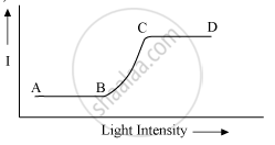
Current AB that flows when no light is incident is called dark current.
-
When photons of light having energy hν fall on the photodiode, more electrons from the valence band move to the conduction band, provided hv is greater than the forbidden energy gap.
-
The current in the circuit increases. As the intensity of light is increased, the current goes on increasing (represented by the part BC).
- When the current does not increase with the increase in intensity of light, the photodiode is said to be saturated. The portion CD of the graph represents the saturated current.
V-I characteristics:
संबंधित प्रश्न
Explain with the help of a diagram, how depletion region and potential barrier are formed in a junction diode.
If a small voltage is applied to a p-n junction diode, how will the barrier potential be affected when it is(ii) reveres biased?
Sunil and his parents were travelling to their village in their car. On the way his mother noticed some grey coloured panels installed on the roof of a low building. She enquired from Sunil what those panels were and Sunil told his mother that those were solar panels.
(a) What were the values displayed by Sunil and his mother? State one value for each.
(b) In what way would the use of solar panels prove to be very useful?
(c) Name the semiconductor device used in solar panels. Briefly explain with the help of a diagram, how this device works
The current in the forward bias is known to be more (~mA) than the current in the reverse bias (~μA). What is the reason, then, to operate the photodiode in reverse bias?
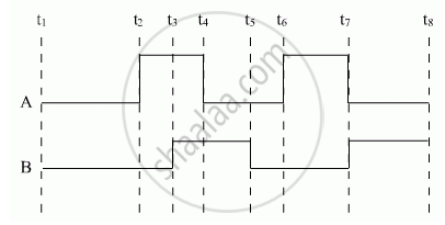
Show the output waveforms (Y) for the following inputs A and B of (i) OR gate (ii) NAND gate ?
With reference to Semiconductor Physics,
Name the process that causes depletion region in a p-n junction.
Pressure P varies as P = `alpha/beta "exp" (- (alpha x)/"k"_"BT")`, where x denotes the distance, kB is the Boltzmann's constant, T is the absolute temperature and α and β are constant. The dimension of β is ______.
Consider the following statements (A) and (B) and identify the correct answer.
- A Zener diode is connected in reverse bias when used as a voltage regulator.
- The potential barrier of the p-n junction lies between 0.1 V to 0.3 V.
The amplifiers X, Y and Z are connected in series. If the voltage gains of X, Y and Z are 10, 20 and 30, respectively and the input signal is 1 mV peak value, then what is the output signal voltage (peak value)
- if dc supply voltage is 10V?
- if dc supply voltage is 5V?
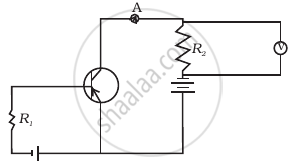
If the resistance R1 is increased (Figure), how will the readings of the ammeter and voltmeter change?