Advertisements
Advertisements
प्रश्न
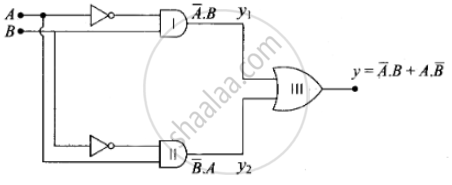
An X-OR gate has following truth table:
| A | B | Y |
| 0 | 0 | 0 |
| 0 | 1 | 1 |
| 1 | 0 | 1 |
| 1 | 1 | 0 |
It is represented by following logic relation `Y = barA.B + A.barB`. Build this gate using AND, OR and NOT gates.
उत्तर
X-OR gate can be realized by the combination of two NOT gates, two AND gates and one OR gate. According to the problem, the logic relation for the given truth table is
When `Y = barA * B + A * barB = Y_1 + Y_2`
`Y_1 = A * B` and `Y_2 = A * barB`
Y1 can be obtained as output of AND gate 1 for which one input is of A through NOT gate and another input is of B. Y2 can be obtained as the output of AND pate II for which one input is of A and the other input is of B through NOT gate.
Now Y can be obtained as output from OR gate, where Y1 and Y2 are inputs of OR gate.
Thus, the logic circuit of this relation is given below.
APPEARS IN
संबंधित प्रश्न
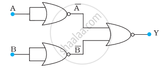
Write the truth table for the circuits given in following figure consisting of NOR gates only. Identify the logic operations (OR, AND, NOT) performed by the two circuits.
(a)
(b)
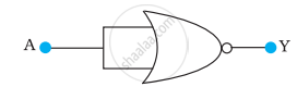
You are given a circuit below. Write its truth table. Hence, identify the logic operation carried out by this circuit. Draw the logic symbol of the gate it corresponds to.

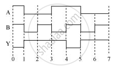
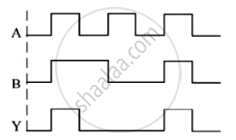
The following figure shows the input waveforms (A, B) and the output waveform (Y) of a gate. Identify the gate, write its truth table and draw its logic symbol.
Let \[X = A \overline{ BC} + B\overline{ CA} + C\overline{AB } .\] Evaluate X for A = B = C = 1.
Show that \[AB + \overline {AB }\] is always 1.
In potential barrier development in a junction diode opposes
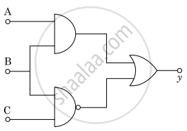
For the given circuit, the input digital signals are applied at terminals A, B, and C. What would be the output at terminal y?
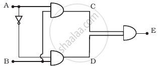
Truth table for the given circuit (Figure) is ______.
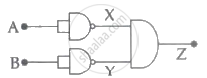
Identify the logic operation carried out by the given circuit:
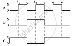
A logic gate circuit has two inputs A and B and output Y. The voltage waveforms of A, B and Y are shown below.
The logic gate circuit is ______.
