Advertisements
Advertisements
प्रश्न
Explain the formation of energy band diagram in case of conductor and semiconductor.
उत्तर
a. Energy band structure in conductor:
1. Conductors are those substances which allow the passage of electric current through them.
2. In a conductor, the valence and conduction energy band overlap each other. Due to this overlapping, a slight P.D across the conductor forces electrons to constitute electric current.
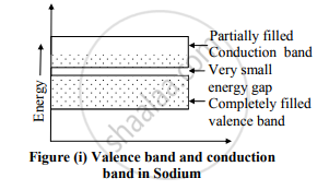
3. In case of sodium, valence band may be completely filled with an extremely small energy gap between them as shown in figure (i).

4. In case of zinc, the valence band is completely filled and the conduction band is empty but the two overlap each other as shown in figure (ii).

5. In both the situations, it can be assumed that there is a single energy band which is partially filled.
Therefore on applying even a small electric field, metals conduct electricity. Thus the electrical behaviour of conductors can be satisfactorily explained by the band energy theory of materials .
b. Energy band structure in semiconductor:

1. In terms of energy bands, we can define semiconductors as those substances, which at room temperature have partially filled conduction band and partially filled valence band with a very narrow energy gap between them. It is less than
3 eV.
2. For Ge, energy gap Eg = 0.7 eV and for Silicon Eg =1.2 eV.
3. At absolute zero, there are no electrons in their conduction band and their valence band is completely filled i.e., at absolute zero, semiconductors like Ge and Si behave like insulators.
4. As the temperature is increased, the energy gap is decreased. Some of the electrons go to the conduction band an d thus the conductivity increases with temperature.
