Advertisements
Advertisements
प्रश्न
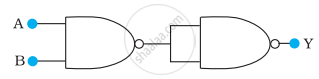
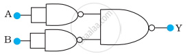
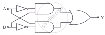
You are given two circuits as shown in following figure, which consist of NAND gates. Identify the logic operation carried out by the two circuits.
(a)
(b)
उत्तर
In both the given circuits, A and B are the inputs and Y is the output.
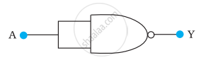
a) The output of the left NAND gate will be `bar("A"."B")`, as shown in the following figure.

Hence, the output of the combination of the two NAND gates is given as:
`"Y" = bar((bar("A.B")).(bar("A.B")))= bar(bar("AB")) + bar(bar("AB")) = "AB"`
Hence, this circuit functions as an AND gate.
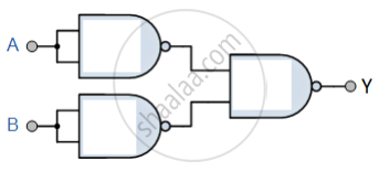
(b) `bar"A"` is the output of the upper left of the NAND gate and `bar"B"` is the output of the lower half of the NAND gate, as shown in the following figure.
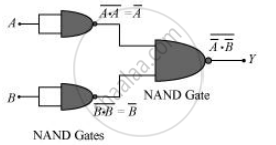
Hence, the output of the combination of the NAND gates will be given as:
`"Y" = bar"A".bar"B" = bar(bar"A") + bar(bar"B") = "A"+"B"`
Hence, this circuit functions as an OR gate.
APPEARS IN
संबंधित प्रश्न
Which logic gate corresponds to the truth table given below?
|
A |
B |
Y |
|
0 |
0 |
I |
|
0 |
1 |
0 |
|
1 |
0 |
0 |
|
1 |
1 |
0 |
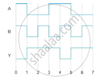
The following figure shows the input waveforms (A, B) and the output waveform (Y) of a gate. Identify the gate, write its truth table and draw its logic symbol.
Write the truth table for a NAND gate connected as given in the following figure.
Hence identify the exact logic operation carried out by this circuit
Give the truth table and circuit symbol for NAND gate
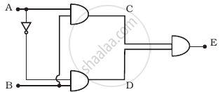
The arrangement given below represents a logic gate :
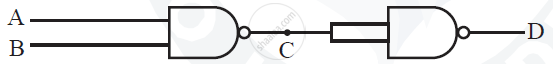
Copy the following truth table in your answer booklet and complete it showing outputs at C
and D.
| A | B | C | D |
| 0 | 0 | ||
| 1 | 0 | ||
| 0 | 1 | ||
| 1 | 0 |
You are given a circuit below. Write its truth table. Hence, identify the logic operation carried out by this circuit. Draw the logic symbol of the gate it corresponds to.

What will be the values of input A and B for the Boolean expression `overline ((A +B) .(A*B)) =1?`
Show that \[AB + \overline {AB }\] is always 1.
Why is the linear portion of the triode characteristic chosen to operate the triode as an amplifier?
Draw the truth table of a NOR gate.
Draw a diagram to show how NAND gates can be combined to obtain an OR gate. (Truth table is not, required)
Useful Constants and Relations:
| 1. | Charge of a proton | (e) | =1.6 × 10⁻¹⁹C |
| 2. | Planck's constant | (h) | = 6·6 × 10-34 Js |
| 3. | Mass of an electron | (m) | = 9·1× 10-31 kg |
| 4. | Permittivity of vacuum | (∈0) | =8 · 85 × 10-12 Fm-1 |
| 5. | `(1/(4pi∈_0))` | =9 ×10⁹ mF-1 | |
| 6. | Permeability of vacuum | (μ0) | = 4π × 10-7 Hm-1 |
| 7. | `((mu_0)/(4pi))` | =1 × 10⁻⁷ Hm-1 | |
| 8. | Speed of light in vacuum | (c) | = 3× 10⁸ ms-1 |
| 9. | Unified atomic mass unit | (u) |
= 931 MeV |
| 10. | Electron volt | (leV) | = 1.6 × 10⁻¹⁹ J |
With the help of a diagram, show how you can use several NAND gates to obtain an OR gate.
Useful Constants and Relations :
| 1. Speed of Light in Vacuum | (c) = 3.00 x 10⁸ m/s |
| 2. Charge of a proton | (e) = 1.60 x 10⁻¹⁹C |
| 3. Planck's Constant | (h) = 6.6 x 10⁻³⁴ Js |
| 4. Permeability of vacuum | (μ0) = 4π x 10-7 Hm-1 |
| 5. Electron Volt | (1eV ) = 1.6 x 10 |
| 6. Unified Atomic Mass Unit | (1u) = 931 MeV |
| (π) = 3.14 | |
| ( ln 2 ) = 0.693 |
You are given a circuit as shown in the figure, which consists of the NAND gate. Identify the logic operation carried out by the two. Write the truth table. Identify the gates equivalent to the tow circuit.
NAND and NOR gates are called universal gates primarily because they ______.
In potential barrier development in a junction diode opposes
The truth table for the following logic circuit is:
Truth table for the given circuit (Figure) is ______.