Advertisements
Advertisements
Question
Consider an npn transistor with its base-emitter junction forward biased and collector base junction reverse biased. Which of the following statements are true?
- Electrons crossover from emitter to collector.
- Holes move from base to collector.
- Electrons move from emitter to base.
- Electrons from emitter move out of base without going to the collector.
Options
d and a
d and a
d and a
d and a
a and b
a and b
a and b
a and b
b and c
b and c
b and c
b and c
a and c
a and c
a and c
a and c
Solution 1
a and c
Explanation:
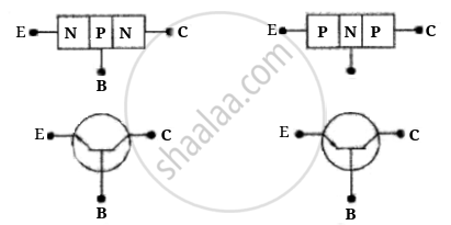
Transistor: A junction transistor is formed by sandwiching 2 thin layer of P-type semiconductors between two N-type semiconductors. or by sandwiching a thin taver of V-type semiconductors between two P-type semiconductors.

E — Emitter (emits majority charge carriers)
C — Collects majority charge carriers
B — Base (provide proper interaction between E and C)

In normal operation base-emitter is forward biased, i.e., the positive pole of the emitter-base battery is connected to the base and its negative pole is connected to the emitter. And collector-base junction is reverse biased, i.e., the positive pole of the collector base battery is connected to the collector and the negative pole to base. Thus, electron moves from emitter to base and crossovers from emitter to collector.
Solution 2
a and c
Explanation:
Transistor: A junction transistor is formed by sandwiching 2 thin layer of P-type semiconductors between two N-type semiconductors. or by sandwiching a thin taver of V-type semiconductors between two P-type semiconductors.

E — Emitter (emits majority charge carriers)
C — Collects majority charge carriers
B — Base (provide proper interaction between E and C)

In normal operation base-emitter is forward biased, i.e., the positive pole of the emitter-base battery is connected to the base and its negative pole is connected to the emitter. And collector-base junction is reverse biased, i.e., the positive pole of the collector base battery is connected to the collector and the negative pole to base. Thus, electron moves from emitter to base and crossovers from emitter to collector.
Solution 3
a and c
Explanation:
Transistor: A junction transistor is formed by sandwiching 2 thin layer of P-type semiconductors between two N-type semiconductors. or by sandwiching a thin taver of V-type semiconductors between two P-type semiconductors.

E — Emitter (emits majority charge carriers)
C — Collects majority charge carriers
B — Base (provide proper interaction between E and C)

In normal operation base-emitter is forward biased, i.e., the positive pole of the emitter-base battery is connected to the base and its negative pole is connected to the emitter. And collector-base junction is reverse biased, i.e., the positive pole of the collector base battery is connected to the collector and the negative pole to base. Thus, electron moves from emitter to base and crossovers from emitter to collector.
Solution 4
a and c
Explanation:
Transistor: A junction transistor is formed by sandwiching 2 thin layer of P-type semiconductors between two N-type semiconductors. or by sandwiching a thin taver of V-type semiconductors between two P-type semiconductors.

E — Emitter (emits majority charge carriers)
C — Collects majority charge carriers
B — Base (provide proper interaction between E and C)

In normal operation base-emitter is forward biased, i.e., the positive pole of the emitter-base battery is connected to the base and its negative pole is connected to the emitter. And collector-base junction is reverse biased, i.e., the positive pole of the collector base battery is connected to the collector and the negative pole to base. Thus, electron moves from emitter to base and crossovers from emitter to collector.
