Advertisements
Advertisements
Question
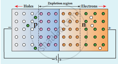
Explain the formation of depletion region and barrier potential in PN junction diode.
Solution

Schematic representation
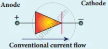
Circuit symbol
1. A p-n junction diode is formed when the p-type semiconductor is fused with an N-type semiconductor.
2. A p-n junction diode is formed when the p-type semiconductor is fused with an N-type semiconductor.
- Forward bias
- Forward bias
a. Forward bias:

- If the positive terminal of the external voltage source is connected to the p-side and the negative terminal to the n-side forward bias takes place.
- Electron moves to n-side holes move to the p side Recombination takes place near the junction and reduces depletion region.
- Electron from n-side accelerates towards p side it experiences reduced potential barrier at the junction.
- Applied voltage is increased, the width of the depletion region and barrier potential further reduced.
- So a large number of electrons pass through the junction.
b. Reverse bias:
- If the positive terminal of the external voltage source is connected to the p-side and the negative terminal to the n-side reverse bias takes place.
- Depletion region is increased potential barrier is also increased.
- Majority of charge carriers from both sides experience a great barrier to cross the junction. So diffusion current reduces.
- The current flows under reverse bias are called reverse saturation current Is.
APPEARS IN
RELATED QUESTIONS
If a positive half-wave rectified voltage is fed to a load resistor, for which part of a cycle there will be current flow through the load?
The zener diode is primarily used as ____________.
The barrier potential of a p-n junction depends on
(i) type of semiconductor material
(ii) amount of doping
(iii) temperature
Which one of the following is correct?
Draw the input and output waveforms of a full wave rectifier.
What is meant by biasing?
Mention the types of biasing.
Explain the construction and working of a full-wave rectifier.
What is an LED? Give the principle of its operation with a diagram.
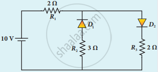
The given circuit has two ideal diodes connected as shown in the figure below. Calculate the current flowing through the resistance R1.
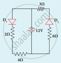
Determine the current flowing through 3 Ω and 4 Ω resistors of the circuit given below. Assume that diodes D1 and D2 are ideal diodes.