Advertisements
Advertisements
Question
Let \[X = A \overline{ BC} + B\overline{ CA} + C\overline{AB } .\] Evaluate X for A = B = C = 0.
Solution
Given:
Output
\[X = A \overline{ BC} + B\overline{ CA} + C\overline{AB } .\]
A = B = C = 0
\[X = 0 . ( \overline{{0 . 0)}} + 0( \overline{{0 . 0)}} + 0 . ( \overline{{0 . 0)}}\]
\[ = 0 . \bar{0} + 0 . \bar{0} + 0 . \bar{0}\]
\[ = 0 . 1 + 0 . 1 + 0 . 1\]
\[ = 0 + 0 + 0\]
\[ = 0\]
APPEARS IN
RELATED QUESTIONS
The output of NOR gate is high, when _______.
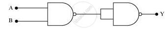
You are given two circuits as shown in following figure, which consist of NAND gates. Identify the logic operation carried out by the two circuits.
(a)
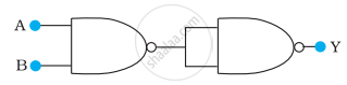
(b)
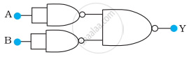
Write the truth table for the circuits given in following figure consisting of NOR gates only. Identify the logic operations (OR, AND, NOT) performed by the two circuits.
(a)
(b)
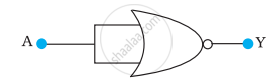
The arrangement given below represents a logic gate :
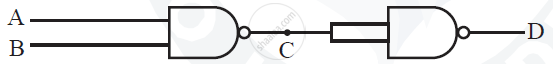
Copy the following truth table in your answer booklet and complete it showing outputs at C
and D.
| A | B | C | D |
| 0 | 0 | ||
| 1 | 0 | ||
| 0 | 1 | ||
| 1 | 0 |
Answer the following question :
Distinguish between digital and analogue signals.
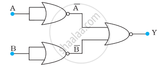
Identify the logic gate represented by the circuit as shown and write its truth table.
What will be the values of input A and B for the Boolean expression `overline ((A +B) .(A*B)) =1?`
An AND gate can be prepared by repetitive use of
(a) NOT gate
(b) OR gate
(c) NAND gate
(d) NOR gate.
Design a logical circuit using AND, OR and NOT gates to evaluate \[A \overline { BC } + B \overline{ CA }\] .
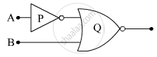
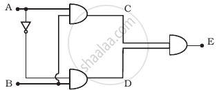
(i) Write the truth tables of the logic gates marked P and Q in the given circuit.
(ii) Write the truth table for the circuit.
NAND and NOR gates are called universal gates primarily because they ______.
The Boolean expression for NAND gate is
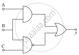
For the given circuit, the input digital signals are applied at terminals A, B, and C. What would be the output at terminal y?
Truth table for the given circuit (Figure) is ______.
An X-OR gate has following truth table:
| A | B | Y |
| 0 | 0 | 0 |
| 0 | 1 | 1 |
| 1 | 0 | 1 |
| 1 | 1 | 0 |
It is represented by following logic relation `Y = barA.B + A.barB`. Build this gate using AND, OR and NOT gates.
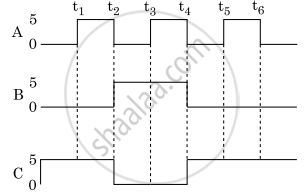
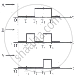
The given figure shows the waveforms for two inputs A and B and that for the output Y of a logic circuit. The logic circuit is ______.
A logic gate circuit has two inputs A and B and output Y. The voltage waveforms of A, B and Y are shown below.
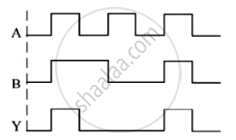
The logic gate circuit is ______.
Which of the following gives a reversible operation?
