Advertisements
Advertisements
Question
With the help of a circuit diagram, explain the workings of a full-wave rectifier.
Solution
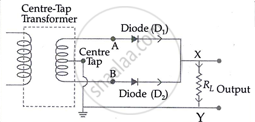
A full-wave rectifier has two diodes arranged in parallel at the terminals of the secondary winding of a centre-tapped step-down transformer. The load resistance RL is linked across the secondary winding and the diodes between points A and B, as seen in the circuit.
End A of the secondary winding becomes positive during the positive half cycle of input a.c., while end B becomes negative. Consequently, diode D1 becomes forward biased, while diode D2 becomes reverse biased. Therefore, diode D1 permits the current to pass through it, whereas diode D2 does not. Consequently, the current in the circuit passes from D1 and through load RL from X to Y.
In the negative half-cycle of the input alternating current, end A of the secondary winding becomes negative and end B becomes positive, resulting in diode D1 being reverse-biased while diode D2 is forward-biased. Diode D1 obstructs current flow, whereas diode D2 permits it, resulting in current traversing from D2 through load RL from point X to point Y.
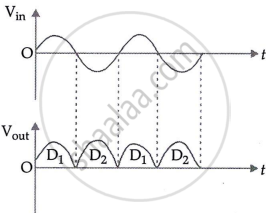
Input-Output waveforms
As the electric current through the load RL flows in the same direction during both half-cycles of the input alternating current, direct current is produced across RL. Although the direction of electric current through an RL circuit remains constant, its magnitude varies over time, so it is referred to as pulsing direct current (d.c.).
