Advertisements
Advertisements
प्रश्न
Answer in detail.
Explain the importance of the depletion region in a p-n junction diode.
उत्तर
- The region across the p-n junction where there are no charges is called the depletion layer or the depletion region.
- During the diffusion of charge carriers across the junction, electrons migrate from the n-side to the p-side of the junction. At the same time, holes are transported from the p-side to the n-side of the junction.
- As a result, in the p-type region near the junction, there are negatively charged acceptor ions, and in the n-type region near the junction, there are positively charged donor ions.
- The potential barrier thus developed, prevents the continuous flow of charges across the junction. A state of electrostatic equilibrium is thus reached across the junction.
- Free charge carriers cannot be present in a region where there is a potential barrier. This creates the depletion region.
- In absence of a depletion region, all the majority charge carriers from the n-region (i.e., electron) will get transferred to the p-region and will get combined with the holes present in that region. This will result in the decreased efficiency of the p-n junction.
- Hence, the formation of a depletion layer across the junction is important to limit the number of majority carriers crossing the junction.
APPEARS IN
संबंधित प्रश्न
Choose the correct option.
A reverse-biased diode is equivalent to:
Choose the correct option.
The potential barrier in p-n diode is due to:
Answer the following question.
What causes a larger current through a p-n junction diode when forward biased?
Explain the I-V characteristic of a forward-biased junction diode.
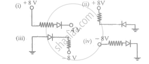
In the following figures, the diodes are either forward biased or reversed biased. Choose the CORRECT statement:

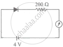
The reading of the ammeter for a silicon diode in the given circuit is:

In case of p-n junction diode, the width of depletion region is ______.
Consider the junction diode as ideal. The value of current flowing through AB is ______.

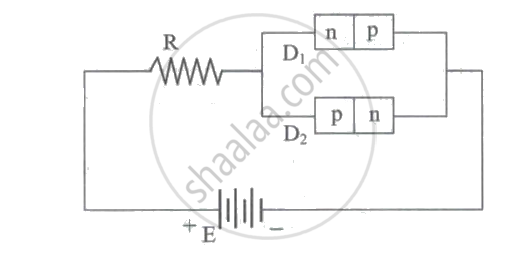
Figure shows two p-n junction diodes along with a resistance R and a dc battery E. The path of flow of appreciable current in the circuit is,

If p - n junction diode is forward biased then ______.
Assuming that the junction diode is ideal, the current in the arrangement shown in

The width of depletion layer of a p-n junction diode, when it is (i) forward biased and (ii) reverse biased respectively ______.
When p-n junction diode is reverse biased, then the width of the barrier potential will ______.
If p-njunction diode is reverse biased then ______.
The region near the junction of an unbiased p-n junction diode is known as depletion layer. The layer is depleted of ______.
In a forward bias arrangement of a p-n junction diode, the ______.
At 0.3 V and 0.7 V, the diodes Ge and Si become conductors respectively. In the given figure, if the ends of diode Ge are overturned, the change in potential V0 will be ______.

