Advertisements
Advertisements
प्रश्न
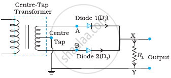
Draw the circuit diagram of a full wave rectifier. Explain its working showing its input and output waveforms.
With the help of a circuit diagram, explain the working of the junction diode as a full wave rectifier. Draw its input and output waveforms.
उत्तर

Figure (a)

(a) A Full-wave rectifier circuit;
(b) Input waveforms given to the diode D1 at A and to the diode D2 at B;
(c) Output waveform across the load RL connected in the full-wave rectifier circuit.
The circuit using two diodes, shown in Fig. (a), gives output rectified voltage corresponding to both the positive as well as negative half of the ac cycle. Hence, it is known as a full-wave rectifier.
Here the p-side of the two diodes is connected to the ends of the secondary of the transformer. The n-side of the diodes is connected together, and the output is taken between this common point of diodes and the midpoint of the secondary transformer. So for a full-wave rectifier, the secondary of the transformer is provided with a centre tapping and so it is called a centre-tap transformer.
As can be seen from Fig. (c) the voltage rectified by each diode is only half the total secondary voltage. Each diode rectifies only for half the cycle, but the two do so for alternate cycles. Thus, the output between their common terminals and the centre tap of the transformer becomes a full-wave rectifier output.
Suppose the input voltage to A with respect to the centre tap at any instant is positive. It is clear that, at that instant, the voltage at B being out of phase will be negative as shown in Fig. (b). So, diode D1 gets forward biased and conducts (while D2 being reverse biased is not conducting). Hence, during this positive half cycle, we get an output current (and an output voltage across the load resistor RL) as shown in Fig. (c).
In the course of the ac cycle when the voltage at A becomes negative with respect to the centre tap, the voltage at B would be positive. In this part of the cycle, diode D1 would not conduct but diode D2 would, giving an output current and output voltage (across RL) during the negative half cycle of the input ac. Thus, we get output voltage during both the positive as well as the negative half of the cycle.
APPEARS IN
संबंधित प्रश्न
When the diode shows saturated current, dynamic place resistance is _____________ .
Explain with a proper diagram how an ac signal can be converted into dc (pulsating) signal with output frequency as double than the input frequency using pn junction diode. Give its input and output waveforms.
The device which uses centre-tapped secondary of the transformer is
A 220 V A.C. supply is connected between points A and B (figure). What will be the potential difference V across the capacitor?

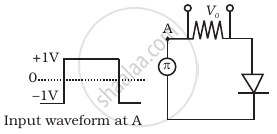
The output of the given circuit in figure is given below.

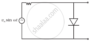
Draw the output waveform across the resistor (Figure).
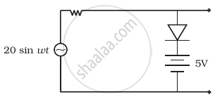
Assuming the ideal diode, draw the output waveform for the circuit given in figure. Explain the waveform.

With the help of a circuit diagram, explain briefly how a p-n junction diode works as a half-wave rectifier.
Give two differences between a half-wave rectifier and a full-wave rectifier.
Draw a labelled circuit diagram of a full wave rectifier. Show graphically how the output voltage varies with time.
