Advertisements
Advertisements
प्रश्न
Draw a circuit diagram of a p-n-p transistor and explain how it works as a transistor amplifier
उत्तर
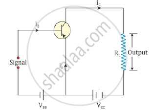
The circuit diagram of a p–n–p transistor is as shown below:

A transistor when operated in the active state acts as an amplifier. The working of a common emitter transistor as an amplifier is based on the principle that a weak input signal given to the base region produces an amplified output signal in the collector region
The circuit diagram for a p–n–p common emitter transistor amplifier can be drawn as shown below:

The battery VBB forward biases the emitter base junction and the battery VCC reverse biases the emitter collector region. The e.m.f. of the batteries should be greater than the barrier potential across base-emitter and collector emitter junction. The output current produces a potential difference across the load resistance RL. A weak alternating signal is applied between the base and the emitter. When the signal increases in the positive direction, the base current also increases. The base current is amplified β times and appears at the collector. The collector current flowing through the collector load resistance produces a voltage. This output voltage is equal to the collector current times the load resistance. Thus, an amplified output is obtained. The voltage gain = output voltage/input voltage.
APPEARS IN
संबंधित प्रश्न
Write the functions of three segments of a transistor.
Draw a circuit diagram of a transistor amplifier in CE configuration.
Define the terms : Input resistance How are these determined using typical input and output characteristics?
Under what condition does the transistor act as an amplifier?
Consider an amplifier circuit using a transistor. The output power is several times greater than the input power. Where does the extra power come from?
Draw a circuit diagram for the common emitter transistor amplifier. What is meant by phase reversal?
Write the truth table of the following circuit. Name the gate represented by this circuit.

In a common base amplifier, the phase difference between the input signal voltage and output voltage is ______.
In common emitter amplifier, the current gain is 62. The collector resistance and input resistance are 5 kΩ and 500 Ω respectively. If the input voltage is 0.01 V, the output voltage is:
A pnp transistor is used in common-emitter mode in an amplifier circuit. A change of 40 µA in the base current brings a change of 2 mA in collector current and 0.04 V in base emitter voltage. Which of the following is the correct value of the input resistor Rin?
