Advertisements
Advertisements
Question
Draw a circuit diagram of a p-n-p transistor and explain how it works as a transistor amplifier
Solution
The circuit diagram of a p–n–p transistor is as shown below:

A transistor when operated in the active state acts as an amplifier. The working of a common emitter transistor as an amplifier is based on the principle that a weak input signal given to the base region produces an amplified output signal in the collector region
The circuit diagram for a p–n–p common emitter transistor amplifier can be drawn as shown below:
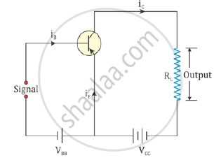
The battery VBB forward biases the emitter base junction and the battery VCC reverse biases the emitter collector region. The e.m.f. of the batteries should be greater than the barrier potential across base-emitter and collector emitter junction. The output current produces a potential difference across the load resistance RL. A weak alternating signal is applied between the base and the emitter. When the signal increases in the positive direction, the base current also increases. The base current is amplified β times and appears at the collector. The collector current flowing through the collector load resistance produces a voltage. This output voltage is equal to the collector current times the load resistance. Thus, an amplified output is obtained. The voltage gain = output voltage/input voltage.
APPEARS IN
RELATED QUESTIONS
For a CE-transistor amplifier, the audio signal voltage across the collector resistance of 2 kΩ is 2 V. Suppose the current amplification factor of the transistor is 100, find the input signal voltage and base current if the base resistance is 1 kΩ.
Draw a circuit diagram for studying the input and output characteristics of a n-p-n transistor in common emitter configuration. Using the circuit, explain how input, output characteristics are obtained
Draw a labelled diagram of a common emitter amplifier, showing waveforms of the signal voltage and output voltage.
Gautam went for a vacation to the village where his grandmother lived. His grandmother took him to watch 'nautanki' one evening. They noticed a blackbox connected to the mike lying nearby. Gautam's grandmother did not know what that box was. When she asked this question to Gautam, he explained to her that it was an amplifier.
(i) Which values were displayed by the grandmother? How can inculcation of these values in students be promoted?
(ii) What is the function of an amplifier?
(iii) Which basic electronic device is used in the amplifier?
Draw a circuit diagram for the common emitter transistor amplifier. What is meant by phase reversal?
Write the truth table of the following circuit. Name the gate represented by this circuit.
In a CE transistor amplifier, the audio signal voltage across the collector resistance of2 kΩ is 2 V If the base resistance is 1 kΩ and the current amplification of the transistor is 100, the input signal voltage is
In common emitter amplifier, the current gain is 62. The collector resistance and input resistance are 5 kΩ and 500 Ω respectively. If the input voltage is 0.01 V, the output voltage is:
A pnp transistor is used in common-emitter mode in an amplifier circuit. A change of 40 µA in the base current brings a change of 2 mA in collector current and 0.04 V in base emitter voltage. Which of the following is the correct value of the input resistor Rin?
When a junction transistor is used as an amplifier in CE-mode,
