Science (English Medium)
Academic Year: 2014-2015
Date: March 2015
Advertisements
Define mobility of a charge carrier
Chapter: [0.02] Electrostatic Potential and Capacitance
Write its (‘mobility’ of charge carriers) S.I. unit
Chapter: [0.03] Current Electricity
In a series LCR circuit, VL = VC ≠ VR. What is the value of power factor?
Chapter: [0.07] Alternating Current
The focal length of an equiconvex lens is equal to the radius of curvature of either face. What is the refractive index of the material of the lens?
Chapter:
Write a relation for polarisation `vecP`of a dielectric material in the presence of an external electric field `vecE .`
Chapter: [0.02] Electrostatic Potential and Capacitance
What happens when a forward bias is applied to a p-n junction?
Chapter: [0.14] Semiconductor Electronics - Materials, Devices and Simple Circuits
Distinguish between ‘Analog’ and ‘Digital’ forms of communication.
Chapter: [0.15] Communication Systems
Explain briefly two commonly used applications of the ‘Internet’.
Chapter: [0.15] Communication Systems
Given the ground state energy E0 = - 13.6 eV and Bohr radius a0 = 0.53 Å. Find out how the de Broglie wavelength associated with the electron orbiting in the ground state would change when it jumps into the first excited state.
Chapter: [0.12] Atoms
State Bohr’s postulate of hydrogen atom which successfully explains the emission lines in the spectrum of hydrogen atom. Use Rydberg formula to determine the wavelength of Hα line. [Given: Rydberg constant R = 1.03 × 10⁷ m−1]
Chapter: [0.12] Atoms
State the two Kirchhoff’s rules used in electric networks. How are there rules justified?
Chapter: [0.03] Current Electricity
Advertisements
Write the important characteristic features by which the interference can be distinguished from the observed diffraction pattern.
Chapter: [0.1] Wave Optics
Explain the basic differences between the construction and working of a telescope and a microscope
Chapter: [0.09] Ray Optics and Optical Instruments
Light of intensity ‘I’ and frequency ‘v’ is incident on a photosensitive surface and causes photoelectric emission. What will be the effect on anode current when (i) the intensity of light is gradually increased. In each case, all other factors remain the same. Explain, giving justification in each case.
Chapter: [0.11] Dual Nature of Radiation and Matter
Light of intensity ‘I’ and frequency ‘v’ is incident on a photosensitive surface and causes photoelectric emission. What will be the effect on anode current when (ii) the frequency of incident radiation is increased. In each case, all other factors remain the same. Explain, giving justification in each case.
Chapter: [0.11] Dual Nature of Radiation and Matter
Light of intensity ‘I’ and frequency ‘v’ is incident on a photosensitive surface and causes photoelectric emission. What will be the effect on anode current when the anode potential is increased? In each case, all other factors remain the same. Explain, giving justification in each case.
Chapter: [0.11] Dual Nature of Radiation and Matter
When is a transistor said to be in active state?
Chapter: [0.14] Semiconductor Electronics - Materials, Devices and Simple Circuits
Draw a circuit diagram of a p-n-p transistor and explain how it works as a transistor amplifier
Chapter: [0.14] Semiconductor Electronics - Materials, Devices and Simple Circuits
Write clearly, why in the case of a transistor (i) the base is thin and lightly doped
Chapter: [0.14] Semiconductor Electronics - Materials, Devices and Simple Circuits
Write clearly, why in the case of a transistor (ii) the emitter is heavily doped.
Chapter: [0.14] Semiconductor Electronics - Materials, Devices and Simple Circuits
State three important factors showing the need for translating a low frequency signal into a high frequency wave before transmission
Chapter: [0.15] Communication Systems
Draw a sketch of a sinusoidal carrier wave along with a modulating signal and show how these are superimposed to obtain the resultant amplitude modulated wave
Chapter: [0.15] Communication Systems
You are given three circuit elements X, Y and Z. When the element X is connected across an a.c. source of a given voltage, the current and the voltage are in the same phase. When the element Y is connected in series with X across the source, voltage is ahead of the current in phase by π/4 . But the current is ahead of the voltage in phase by π/4when Z is connected in series with X across the source. Identify the circuit elements X, Y and Z. When all the three elements are connected in series across the same source, determine the impedance of the circuit.Draw a plot of the current versus the frequency of applied source and mention the significance of this plot.
Chapter: [0.07] Alternating Current
plot a graph showing the variation of current density (j) versus the electric field (E) for two conductors of different materials. What information from this plot regarding the properties of the conducting material, can be obtained which can be used to select suitable materials for use in making (i) standard resistance and (ii) connecting wires in electric circuits?
Chapter: [0.01] Electric Charges and Fields
Electron drift speed is estimated to be of the order of mm s−1. Yet large current of the order of few amperes can be set up in the wire. Explain briefly.
Chapter: [0.04] Moving Charges and Magnetism
State Biot – Savart law.
Chapter: [0.04] Moving Charges and Magnetism
Deduce the expression for the magnetic field at a point on the axis of a current carrying circular loop of radius ‘R’ distant ‘x’ from the centre. Hence, write the magnetic field at the centre of a loop.
Chapter: [0.04] Moving Charges and Magnetism
What dose a polaroid consist of?
Chapter: [0.1] Wave Optics
Show, using a simple polaroid, that light waves are transverse in nature. Intensity of light coming out of a polaroid does not change irrespective of the orientation of the pass axis of the polaroid. Explain why.
Chapter: [0.1] Wave Optics
How is a Zener diode fabricated?
Chapter: [0.14] Semiconductor Electronics - Materials, Devices and Simple Circuits
What causes the setting up of high electric field even for small reverse bias voltage across the diode?
Chapter: [0.14] Semiconductor Electronics - Materials, Devices and Simple Circuits
Describe, with the help of a circuit diagram, the working of Zener diode as a voltage regulator.
Chapter: [0.14] Semiconductor Electronics - Materials, Devices and Simple Circuits
Explain with the help of a diagram, how depletion region and potential barrier are formed in a junction diode.
Chapter: [0.14] Semiconductor Electronics - Materials, Devices and Simple Circuits
If a small voltage is applied to a p-n junction diode, how will the barrier potential be affected when it is (i) forward biased
Chapter: [0.14] Semiconductor Electronics - Materials, Devices and Simple Circuits
If a small voltage is applied to a p-n junction diode, how will the barrier potential be affected when it is(ii) reveres biased?
Chapter: [0.14] Semiconductor Electronics - Materials, Devices and Simple Circuits
Advertisements
Arrange the following electromagnetic wave in the order of their increasing wavelength:
(a) γ- rays
(b) Microwaves
(c) X-rays
(d) Radio waves
Chapter: [0.08] Electromagnetic Waves
How are infrared waves produced?
Chapter: [0.08] Electromagnetic Waves
What role dose infra-red radiation play in maintain the Earth’s warmth
Chapter: [0.08] Electromagnetic Waves
What role dose infra-red radiation play in physical therapy?
Chapter: [0.08] Electromagnetic Waves
Explain briefly the process of charging a parallel plate capacitor when it is connected across a d.c. battery
Chapter: [0.02] Electrostatic Potential and Capacitance
A capacitor of capacitance ‘C’ is charged to ‘V’ volts by a battery. After some time the battery is disconnected and the distance between the plates is doubled. Now a slab of dielectric constant, 1 < k < 2, is introduced to fill the space between the plates. How will the following be affected? (a) The electric field between the plates of the capacitor Justify your answer by writing the necessary expressions.
Chapter: [0.02] Electrostatic Potential and Capacitance
A capacitor of capacitance ‘C’ is charged to ‘V’ volts by a battery. After some time the battery is disconnected and the distance between the plates is doubled. Now a slab of dielectric constant, 1 < k < 2, is introduced to fill the space between the plates. How will the following be affected? (b) The energy stored in the capacitor Justify your answer by writing the necessary expressions
Chapter: [0.02] Electrostatic Potential and Capacitance
Write symbolically the nuclear β+ decay process of `""_6^11C` Is the decayed product X an isotope or isobar of (`""_6^11C`)? Given the mass values m (`""_6^11C`) = 11.011434 u and m (X) = 11.009305 u. Estimate the Q-value in this process.
Chapter: [0.13] Nuclei
An object is placed 15 cm in front of a convex lens of focal length 10 cm. Find the nature and position of the image formed. Where should a concave mirror of radius of curvature 20 cm be placed so that the final image is formed at the position of the object itself?
Chapter: [0.09] Ray Optics and Optical Instruments
Ajit had a high tension tower erected on his farm land. He kept complaining to the authorities to remove it as it was occupying a large portion of his land. His uncle, who was a teacher, explained to him the need for erecting these towers for efficient transmission of power. As Ajit realised its significance, he stopped complaining.
Answer the following questions:
(a) Why is it necessary to transport power at high voltage?
(b) A low power factor implies large power loss. Explain.
(c) Write two values each displayed by Ajit and his uncle.
Chapter: [0.07] Alternating Current
Deduce the expression for the potential energy of a system of two charges q1 and q2 located `vec(r_1)` and `vec(r_2)`, respectively, in an external electric field.
Chapter: [0.02] Electrostatic Potential and Capacitance
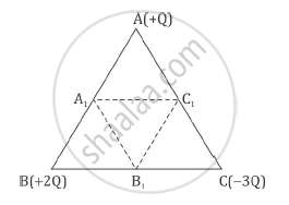
Three point charges, + Q + 2Q and – 3Q are placed at the vertices of an equilateral triangle ABC of side l. If these charges are displaced to the mid-point A1, B1 and C1, respectively, find the amount of the work done in shifting the charges to the new locations.
Chapter: [0.02] Electrostatic Potential and Capacitance
Define electric flux.
Chapter: [0.01] Electric Charges and Fields
Write its (electric flux.) S.I unit.
Chapter: [0.01] Electric Charges and Fields
State and explain Gauss’s law.
Chapter: [0.01] Electric Charges and Fields
Find out the outward flux to a point charge +q placed at the centre of a cube of side ‘a’. Why is it found to be independent of the size and shape of the surface enclosing it? Explain.
Chapter: [0.01] Electric Charges and Fields
Obtain an expression for the energy stored in a solenoid of self-inductance ‘L’ when the current through it grows from zero to ‘I’.
Chapter: [0.04] Moving Charges and Magnetism
A square loop MNOP of side 20 cm is placed horizontally in a uniform magnetic field acting vertically downwards as shown in the figure. The loop is pulled with a constant velocity of 20 cm s−1 till it goes out of the field.
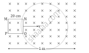
(i) Depict the direction of the induced current in the loop as it goes out of the field. For how long would the current in the loop persist?
(ii) Plot a graph showing the variation of magnetic flux and induced emf as a function of time.
Chapter: [0.06] Electromagnetic Induction
Draw the magnetic field lines due to a circular loop area `vecA` carrying current I. Show that it acts as a bar magnet of magnetic moment `vecm = IvecA .`
Chapter: [0.05] Magnetism and Matter
Derive the expression for the magnetic field due to a solenoid of length ‘2l’, radius ‘a’ having ’n’ number of turns per unit length and carrying a steady current ‘I’ at a point
on the axial line, distance ‘r’ from the centre of the solenoid. How does this expression compare with the axial magnetic field due to a bar magnet of magnetic moment ‘m’?
Chapter: [0.04] Moving Charges and Magnetism
In young’s double slit experiment, deduce the conditions for obtaining constructive and destructive interference fringes. Hence, deduce the expression for the fringe width.
Chapter: [0.1] Wave Optics
Show that the fringe pattern on the screen is actually a superposition of slit diffraction from each slit.
Chapter: [0.1] Wave Optics
What should be the width of each slit to obtain 10 maxima of the double slit pattern within the central maximum of the single slit pattern, for green light of wavelength 500 nm, if the separation between two slits is 1 mm?
Chapter: [0.1] Wave Optics
Two thin convex lenses L1 and L2 of focal lengths f1 and f2, respectively, are placed coaxially in contact. An object is placed at a point beyond the focus of lens L1. Draw a ray diagram to show the image formation by the combination and hence derive the expression for the focal length of the combined system.
Chapter: [0.09] Ray Optics and Optical Instruments
A ray PQ incident on the face AB of a prism ABC, as shown in the figure, emerges from the face AC such that AQ = AR.
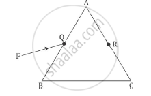
Draw the ray diagram showing the passage of the ray through the prism. If the angle of the prism is 60° and refractive index of the material of prism is `sqrt3` , determine the values of angle of incidence and angle of deviation
Chapter: [0.09] Ray Optics and Optical Instruments
Other Solutions
Submit Question Paper
Help us maintain new question papers on Shaalaa.com, so we can continue to help studentsonly jpg, png and pdf files
CBSE previous year question papers Class 12 Physics with solutions 2014 - 2015
Previous year Question paper for CBSE Class 12 Physics-2015 is solved by experts. Solved question papers gives you the chance to check yourself after your mock test.
By referring the question paper Solutions for Physics, you can scale your preparation level and work on your weak areas. It will also help the candidates in developing the time-management skills. Practice makes perfect, and there is no better way to practice than to attempt previous year question paper solutions of CBSE Class 12.
How CBSE Class 12 Question Paper solutions Help Students ?
• Question paper solutions for Physics will helps students to prepare for exam.
• Question paper with answer will boost students confidence in exam time and also give you an idea About the important questions and topics to be prepared for the board exam.
• For finding solution of question papers no need to refer so multiple sources like textbook or guides.
