Advertisements
Advertisements
Questions
Explain with the help of a diagram, how depletion region and potential barrier are formed in a junction diode.
State briefly the processes involved in the formation of p-n junction explaining clearly how the depletion region is formed.
Solution 1
We know that in an n-type semiconductor, the concentration of electrons is more compared to the concentration of holes. Similarly, in a p-type semiconductor, the concentration of holes is more than the concentration of electrons

During the formation of a p–n junction and because of the concentration gradient across the p and n sides, holes diffuse from the p-side to the n-side (p → n) and electrons diffuse from the n-side to the p-side (n → p). This motion of charge gives rise to a diffusion current across the junction. When an electron diffuses from n → p, it leaves behind an ionised donor on the n-side. This ionised donor (positive charge) is immobile as it is bonded to the surrounding atoms. As the electrons continue to diffuse from n → p, a layer of positive charge (or positive space–charge region) on nside of the junction is developed. Similarly, when a hole diffuses from p → n due to the concentration gradient, it leaves behind an ionised acceptor (negative charge) which is immobile. As the holes continue to diffuse, a layer of negative charge (or negative space–charge region) on the p-side of the junction is developed. This space–charge region on either side of the junction together is known as the
depletion region.
Because of the positive space–charge region on the n-side of the junction and negative space charge region on the p-side of the junction, an electric field directed from the positive charge towards the negative charge develops. Due to this field, an electron on the p-side of the junction moves to the n-side and a hole on the n-side of the junction moves to the p-side. The loss of electrons from the n-region and the gain of electrons by the p-region cause a difference of potential across the junction of the two regions. This is how the barrier potential is formed.
Solution 2
As we know that n-type semi-conductor has more concentration of electrons than that of a hole and p-type semi-conductor has more concentration of holes than an electron. Due to the difference in concentration of charge carriers in the two regions of p-n junction, the holes diffuse from p-side to n-side and electrons diffuse from n-side to p-side.
When an electron diffuses from n to p, it leaves behind it an ionised donor on n-side. The ionised donor (+ ve charge) is immobile as it is bound by the surrounding atoms. Therefore, a layer of positive charge is developed on the n-side of the junction. Similarly, a layer of negative charge is developed on the p-side

Hence, a space-charge region is formed on either side of the junction, which has immobile ions and is devoid of any charge carrier, called as depletion layer or depletion region
APPEARS IN
RELATED QUESTIONS
Meeta's father was driving her to school. At the traffic signal, she noticed that each traffic light was made of many tiny lights instead of a single bulb. When Meeta asked this question to her father, he explained the reason for this.
Answer the following questions based on above information:
(i) What were the values displayed by Meeta and her father?
(ii) What answer did Meeta's father give?
(iii) What are the tiny lights in traffic signals called and how do these operate?
A p-n photodiode is fabricated from a semiconductor with band gap of 2.8 eV. Can it detect a wavelength of 6000 nm?
How is a photodiode fabricated?
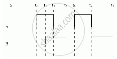
Show the output waveforms (Y) for the following inputs A and B of (i) OR gate (ii) NAND gate ?

The plate resistance of a triode is 8 kΩ and the transconductance is 2.5 millimho. (a) If the plate voltage is increased by 48 V and the grid voltage is kept constant, what will be the increase in the plate current? (b) With plate voltage kept constant at this increased value, by how much should the grid voltage be decreased in order to bring the plate current back to its initial value?
What is a solar cell?
Explain photodiode.
Draw solar cells of I-V characteristics.
Draw the circuit diagram of an illuminated photodiode and its I-V characteristics.
What energy conversion takes place in a solar cell?
