Advertisements
Advertisements
प्रश्न
Explain with the help of a diagram, how depletion region and potential barrier are formed in a junction diode.
State briefly the processes involved in the formation of p-n junction explaining clearly how the depletion region is formed.
उत्तर १
We know that in an n-type semiconductor, the concentration of electrons is more compared to the concentration of holes. Similarly, in a p-type semiconductor, the concentration of holes is more than the concentration of electrons

During the formation of a p–n junction and because of the concentration gradient across the p and n sides, holes diffuse from the p-side to the n-side (p → n) and electrons diffuse from the n-side to the p-side (n → p). This motion of charge gives rise to a diffusion current across the junction. When an electron diffuses from n → p, it leaves behind an ionised donor on the n-side. This ionised donor (positive charge) is immobile as it is bonded to the surrounding atoms. As the electrons continue to diffuse from n → p, a layer of positive charge (or positive space–charge region) on nside of the junction is developed. Similarly, when a hole diffuses from p → n due to the concentration gradient, it leaves behind an ionised acceptor (negative charge) which is immobile. As the holes continue to diffuse, a layer of negative charge (or negative space–charge region) on the p-side of the junction is developed. This space–charge region on either side of the junction together is known as the
depletion region.
Because of the positive space–charge region on the n-side of the junction and negative space charge region on the p-side of the junction, an electric field directed from the positive charge towards the negative charge develops. Due to this field, an electron on the p-side of the junction moves to the n-side and a hole on the n-side of the junction moves to the p-side. The loss of electrons from the n-region and the gain of electrons by the p-region cause a difference of potential across the junction of the two regions. This is how the barrier potential is formed.
उत्तर २
As we know that n-type semi-conductor has more concentration of electrons than that of a hole and p-type semi-conductor has more concentration of holes than an electron. Due to the difference in concentration of charge carriers in the two regions of p-n junction, the holes diffuse from p-side to n-side and electrons diffuse from n-side to p-side.
When an electron diffuses from n to p, it leaves behind it an ionised donor on n-side. The ionised donor (+ ve charge) is immobile as it is bound by the surrounding atoms. Therefore, a layer of positive charge is developed on the n-side of the junction. Similarly, a layer of negative charge is developed on the p-side

Hence, a space-charge region is formed on either side of the junction, which has immobile ions and is devoid of any charge carrier, called as depletion layer or depletion region
APPEARS IN
संबंधित प्रश्न
If a small voltage is applied to a p-n junction diode, how will the barrier potential be affected when it is(ii) reveres biased?
With what considerations in view, a photodiode is fabricated? State its working with the help of a suitable diagram.
Even though the current in the forward bias is known to be more than in the reverse bias, yet the photodiode works in reverse bias. What is the reason?
Write briefly the important processes that occur during the formation of p−n junction. With the help of necessary diagrams, explain the term 'barrier potential'.
Draw the circuit diagram of a full wave rectifier using p-n junction diode.
Explain its working and show the output, input waveforms.
How does a light emitting diode (LED) work? Give two advantages of LED’s over the conventional incandescent lamps.
What happens to the width of depletion player of a p-n junction when it is (i) forward biased, (ii) reverse biased?
Explain how a potential barrier is developed in a p-n junction diode.
A p-n photodiode is fabricated from a semiconductor with a band gap of 2.5 eV. lt can detect a signal of wavelength ______.
In Figure, assuming the diodes to be ideal ______.

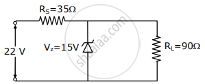
The value of power dissipated across the Zener diode (Vz = 15 V) connected in the circuit as shown in the figure is x × 10–1 watt. The value of x, to the nearest integer, is ______.

