Advertisements
Advertisements
प्रश्न
In Figure, assuming the diodes to be ideal ______.

पर्याय
D1 is forward biased and D2 is reverse biased and hence current flows from A to B.
D2 is forward biased and D1 is reverse biased and hence no current flows from B to A and vice versa.
D1 and D2 are both forward biased and hence current flows from A to B.
D1 and D2 are both reverse biased and hence no current flows from A to B and vice versa.
उत्तर
In Figure, assuming the diodes to be ideal D2 is forward biased and D1 is reverse biased and hence no current flows from B to A and vice versa.
Explanation:

A symbol of the diode is represented like this: In this problem first, we have to check the polarity of the diodes. –10 V is the lower voltage in the circuit. Now p-side of p-n Anode Cathode junction D1 is connected to lower voltage and n-side of D1 to the higher voltage. Thus D1 is reverse biased.
Now, let us analyse 2nd diode of the given circuit. The p-side of p-n junction D2 is at higher potential and n-side of D2 is at lower potential. Therefore D2 is forward biased.
Hence, the current flows through the junction from B to A.
APPEARS IN
संबंधित प्रश्न
Carbon, silicon and germanium have four valence electrons each. These are characterised by valence and conduction bands separated by energy band gap respectively equal to (Eg)C, (Eg)Si and (Eg)Ge. Which of the following statements is true?
Write briefly the important processes that occur during the formation of p−n junction. With the help of necessary diagrams, explain the term 'barrier potential'.
How is a photodiode fabricated?
Briefly explain its working. Draw its V - I characteristics for two different intensities of illumination ?
How does a light emitting diode (LED) work? Give two advantages of LED’s over the conventional incandescent lamps.
Explain the formation of depletion layer and potential barrier in a p−n junction.
A p-n photodiode is fabricated from a semiconductor with a band gap of 2.5 eV. lt can detect a signal of wavelength ______.
The amplifiers X, Y and Z are connected in series. If the voltage gains of X, Y and Z are 10, 20 and 30, respectively and the input signal is 1 mV peak value, then what is the output signal voltage (peak value)
- if dc supply voltage is 10V?
- if dc supply voltage is 5V?
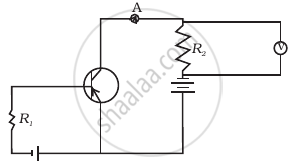
If the resistance R1 is increased (Figure), how will the readings of the ammeter and voltmeter change?

Draw solar cells of I-V characteristics.
