Advertisements
Advertisements
प्रश्न
The amplifiers X, Y and Z are connected in series. If the voltage gains of X, Y and Z are 10, 20 and 30, respectively and the input signal is 1 mV peak value, then what is the output signal voltage (peak value)
- if dc supply voltage is 10V?
- if dc supply voltage is 5V?
उत्तर
Total voltage amplification is defined as the ratio of output signal voltage and input signal voltage.
According to the problem. voltage gain in X, vx = 10
Voltage gain in Y, vy = 20
Voltage gain in Z, vz = 30
ΔV1 = 1 mV = 10–3 V
And Total voltage amplification = vx × vy × vz
ΔV0 = vx × vy × vz × ΔV1
= 10 × 20 × 30 ×10–3 = 6V
- If DC supply voltage is 10 V, then output is 6 V, since the theoretical gain is equal to practical gain, i.e., the output can never be greater than 6 V.
- If DC supply voltage is 5 V, i.e., Vcc = 5 V. Then, the output peak will not exceed 5 V. Hence V0 = 5 V.
APPEARS IN
संबंधित प्रश्न
Meeta's father was driving her to school. At the traffic signal, she noticed that each traffic light was made of many tiny lights instead of a single bulb. When Meeta asked this question to her father, he explained the reason for this.
Answer the following questions based on above information:
(i) What were the values displayed by Meeta and her father?
(ii) What answer did Meeta's father give?
(iii) What are the tiny lights in traffic signals called and how do these operate?
Using the necessary circuit diagrams, show how the V-I characteristics of a p-n junction are obtained in
Forward biasing
How are these characteristics made use of in rectification?
The width of depletion region of p-n junction diode is _______.
(A) 0.5 nm to 1 nm
(B) 5 nm to 10 nm
(C) 50 nm to 500 nm
(D) 500 nm to 1000 nm
Write briefly the important processes that occur during the formation of p−n junction. With the help of necessary diagrams, explain the term 'barrier potential'.
How is a photodiode fabricated?
Write the important considerations which are to be taken into account while fabricating a p-n junction diode to be used as a Light Emitting Diode (LED). What should be the order of the band gap of an LED, if it is required to emit light in the visible range? Draw a circuit diagram and explain its action.
Which one of the following is not the advantage of LED?
Consider the following statements (A) and (B) and identify the correct answer.
- A Zener diode is connected in reverse bias when used as a voltage regulator.
- The potential barrier of the p-n junction lies between 0.1 V to 0.3 V.
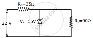
The value of power dissipated across the Zener diode (Vz = 15 V) connected in the circuit as shown in the figure is x × 10–1 watt. The value of x, to the nearest integer, is ______.

What energy conversion takes place in a solar cell?
