Advertisements
Advertisements
प्रश्न
Write briefly the important processes that occur during the formation of p−n junction. With the help of necessary diagrams, explain the term 'barrier potential'.
उत्तर
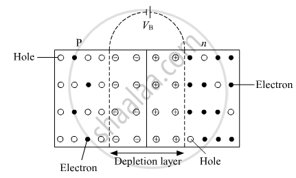
A thin p-type semiconductor wafer is taken and a part of it is converted into n-si by adding a small quantity of pentavalent impurity. The wafer now contains a p-region and an n-region and a metallurgical junction between p and n region.
The n-type semiconductor has more concentration of electrons than hole and p-type semiconductor has more concentration of holes than electrons. So, the holes diffuse from the p-side to the n-side and electrons diffuse from the n-side to the p-side. When an electron diffuses from the n-side to the p-side, it leaves an ionised donor behind it in the n-region. The ionised donor, which is positively charged, is immobile as it is bounded by surrounding atoms. Therefore, a layer of positive charge is developed on n-side of the junction. Similarly, when holes diffuse from p-side to n-side, they leave an ionised acceptor behind them in the p-region. The ionised acceptor, which is negatively charged, is also immobile due to surrounding atoms. Thus, a layer of negative charge is developed on the p-side of the junction.
This space region on both the sides of p-n junction, devoid of any charge carrier, will form a region called depletion region.

Due to the positive charge region on n-side of the junction and negative charge on p-side of the junction, an electric electric field is set up across the junction from the positive charge towards the negative charge. This electric field sets up a barrier potential at the junction that opposes diffusion of majority charge carriers into opposite regions. As the diffusion process continues, the space-charge regions across the junction extend. The strength of the electric field increases; thereby, increasing the drift current . This process continues until the diffusion current becomes equal to the drift current. When this stage is reached, the movement of majority carriers across the junction stops. Now the junction is in equilibrium state. At this stage, the potential barrier across the p-n junction has maximum value \[V_B\].
It means that he barrier voltage stops the diffusion of majority charge carriers from p- to n-region across the junction and vice versa. This potential acts as a barrier and, hence, is known as barrier potential.
APPEARS IN
संबंधित प्रश्न
If a small voltage is applied to a p-n junction diode, how will the barrier potential be affected when it is(ii) reveres biased?
With what considerations in view, a photodiode is fabricated? State its working with the help of a suitable diagram.
Even though the current in the forward bias is known to be more than in the reverse bias, yet the photodiode works in reverse bias. What is the reason?
Using the necessary circuit diagrams, show how the V-I characteristics of a p-n junction are obtained in
Forward biasing
How are these characteristics made use of in rectification?
Carbon, silicon and germanium have four valence electrons each. These are characterised by valence and conduction bands separated by energy band gap respectively equal to (Eg)C, (Eg)Si and (Eg)Ge. Which of the following statements is true?
A p-n photodiode is fabricated from a semiconductor with band gap of 2.8 eV. Can it detect a wavelength of 6000 nm?
Why is zener diode fabricated by heavily doping both p- and n-sides of the junction?
Draw the circuit diagram of a full wave rectifier using p-n junction diode.
Explain its working and show the output, input waveforms.
Read the following paragraph and answer the questions.
|
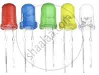
LED is a heavily doped P-N junction which under forward bias emits spontaneous radiation. When it is forward-biased, due to recombination of holes and electrons at the junction, energy is released in the form of photons. In the case of Si and Ge diode, the energy released in recombination lies in the infrared region. LEDs that can emit red, yellow, orange, green and blue light are commercially available. The semiconductor used for fabrication of visible LEDs must at least have a band gap of 1.8 eV. The compound semiconductor Gallium Arsenide – Phosphide is used for making LEDs of different colours.
|
- Why are LEDs made of compound semiconductor and not of elemental semiconductors?
- What should be the order of bandgap of an LED, if it is required to emit light in the visible range?
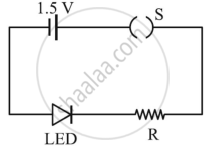
- A student connects the blue coloured LED as shown in the figure. The LED did not glow when switch S is closed. Explain why?

OR
iii. Draw V-I characteristic of a p-n junction diode in
(i) forward bias and (ii) reverse bias
Briefly explain how emf is generated in a solar cell.
Draw solar cells of I-V characteristics.

