Advertisements
Advertisements
प्रश्न
Draw the circuit diagram of a full wave rectifier using p-n junction diode.
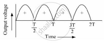
Explain its working and show the output, input waveforms.
उत्तर


Full wave rectifier:
When the diode rectifies the whole of the AC wave, it is called full wave rectifier.
The figure shows the arrangement for using diode as full wave rectifier. The alternating input signal is fed to the primary P1P2 of a transformer. The output signal appears across the load resistance RL.
During the positive half of the input signal, suppose P1 and P2 are negative and positive respectively. This would mean that S1 and S2 are positive and negative respectively. Therefore, the diode D1 is forward biased and D2 is reverse biased. The flow of current in the load resistance RL is from A to B.
During the negative half of the input signal, S1 and S2 are negative and positive respectively. Therefore, the diode D1 is reverse biased and D2 is forward biased. The flow of current in the load resistance RL is from A to B.
APPEARS IN
संबंधित प्रश्न
Colour of light emitted by LED depends upon__________________ .
- its forward bias
- its reverse bias
- the band gap of the material of semiconductor
- its size
If a small voltage is applied to a p-n junction diode, how will the barrier potential be affected when it is (i) forward biased
Describe, with the help of a circuit diagram, the working of a photodiode.
Explain the formation of depletion layer and potential barrier in a p−n junction.
The plate resistance of a triode is 8 kΩ and the transconductance is 2.5 millimho. (a) If the plate voltage is increased by 48 V and the grid voltage is kept constant, what will be the increase in the plate current? (b) With plate voltage kept constant at this increased value, by how much should the grid voltage be decreased in order to bring the plate current back to its initial value?
Write the important considerations which are to be taken into account while fabricating a p-n junction diode to be used as a Light Emitting Diode (LED). What should be the order of band gap of an LED, if it is required to emit light in the visible range? Draw a circuit diagram and explain its action.
What is the magnitude of the potential barrier across a Ge p-n junction?
Pressure P varies as P = `alpha/beta "exp" (- (alpha x)/"k"_"BT")`, where x denotes the distance, kB is the Boltzmann's constant, T is the absolute temperature and α and β are constant. The dimension of β is ______.
A p-n photodiode is fabricated from a semiconductor with a band gap of 2.5 eV. lt can detect a signal of wavelength ______.
What energy conversion takes place in a solar cell?
