Advertisements
Advertisements
प्रश्न
The plate resistance of a triode is 8 kΩ and the transconductance is 2.5 millimho. (a) If the plate voltage is increased by 48 V and the grid voltage is kept constant, what will be the increase in the plate current? (b) With plate voltage kept constant at this increased value, by how much should the grid voltage be decreased in order to bring the plate current back to its initial value?
उत्तर
Given:-
Plate resistance,
`r_p=8KOmega=8000kOmega`
Change in plate voltage,
`deltaV_p=48V`
Formula for plate resistance:
\[r_P = \left( \frac{\delta V_P}{\delta I_P} \right)_{V_G = \text{constant}} \]
\[ \Rightarrow \delta I_p = \frac{\delta V_p}{r_p} {}_{V_{G = \text{constant}}} \]
\[ \Rightarrow \delta I_p = \frac{48}{8000} = 0 . 006 A = 6 \text{ mA}\]
(b) Now, Vp is kept constant.
Change in plate current,
`deltaI_p=6"mA"=0.006A`
Trasconductance,
\[g_m = 0 . 0025 mho\]
\[\delta V_G = \frac{\delta I_p}{g_m} = \frac{0 . 006}{0 . 0025}\]
\[\delta V_G = 2 . 4 V, \text{ at constant plate voltage}\]
APPEARS IN
संबंधित प्रश्न
How is a Zener diode fabricated?
Explain with the help of a diagram, how depletion region and potential barrier are formed in a junction diode.
If a small voltage is applied to a p-n junction diode, how will the barrier potential be affected when it is (i) forward biased
If a small voltage is applied to a p-n junction diode, how will the barrier potential be affected when it is(ii) reveres biased?
Using the necessary circuit diagrams, show how the V-I characteristics of a p-n junction are obtained in
Forward biasing
How are these characteristics made use of in rectification?
Write briefly the important processes that occur during the formation of p−n junction. With the help of necessary diagrams, explain the term 'barrier potential'.
How is a photodiode fabricated?
Describe briefly, with the help of a diagram, the role of the two important processes involved in the formation of a p-n junction ?
What happens to the width of depletion player of a p-n junction when it is (i) forward biased, (ii) reverse biased?
Draw the circuit arrangement for studying the V-I characteristics of a p-n junction diode in reverse bias. Plot the V-I characteristics in this case.
Draw the V-I characteristics of an LED. State two advantages of LED lamps over convertional incandescent lamps.
Choose the correct answer from given options
The wavelength and intensity of light emitted by a LED depend upon
Pressure P varies as P = `alpha/beta "exp" (- (alpha x)/"k"_"BT")`, where x denotes the distance, kB is the Boltzmann's constant, T is the absolute temperature and α and β are constant. The dimension of β is ______.
For LED's to emit light in visible region of electromagnetic light, it should have energy band gap in the range of:
Why a photo-diode is operated in reverse bias whereas the current in the forward bias is much larger than that in the reverse bias? Explain. Mention its two uses.
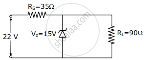
The value of power dissipated across the Zener diode (Vz = 15 V) connected in the circuit as shown in the figure is x × 10–1 watt. The value of x, to the nearest integer, is ______.

What energy conversion takes place in a solar cell?
