Advertisements
Advertisements
प्रश्न
What happens to the width of depletion player of a p-n junction when it is (i) forward biased, (ii) reverse biased?
उत्तर
(i) In forward bias, the width of the depletion layer decreases.
(ii) In reverse bias, the width of the depletion layer increases.
APPEARS IN
संबंधित प्रश्न
Explain with the help of a diagram, how depletion region and potential barrier are formed in a junction diode.
If a small voltage is applied to a p-n junction diode, how will the barrier potential be affected when it is (i) forward biased
If a small voltage is applied to a p-n junction diode, how will the barrier potential be affected when it is(ii) reveres biased?
Carbon, silicon and germanium have four valence electrons each. These are characterised by valence and conduction bands separated by energy band gap respectively equal to (Eg)C, (Eg)Si and (Eg)Ge. Which of the following statements is true?
Draw the circuit diagram of a full wave rectifier using p-n junction diode.
Explain its working and show the output, input waveforms.
With reference to Semiconductor Physics,
Name the process that causes depletion region in a p-n junction.
The amplifiers X, Y and Z are connected in series. If the voltage gains of X, Y and Z are 10, 20 and 30, respectively and the input signal is 1 mV peak value, then what is the output signal voltage (peak value)
- if dc supply voltage is 10V?
- if dc supply voltage is 5V?
Read the following paragraph and answer the questions.
|
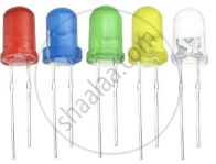
LED is a heavily doped P-N junction which under forward bias emits spontaneous radiation. When it is forward-biased, due to recombination of holes and electrons at the junction, energy is released in the form of photons. In the case of Si and Ge diode, the energy released in recombination lies in the infrared region. LEDs that can emit red, yellow, orange, green and blue light are commercially available. The semiconductor used for fabrication of visible LEDs must at least have a band gap of 1.8 eV. The compound semiconductor Gallium Arsenide – Phosphide is used for making LEDs of different colours.
|
- Why are LEDs made of compound semiconductor and not of elemental semiconductors?
- What should be the order of bandgap of an LED, if it is required to emit light in the visible range?
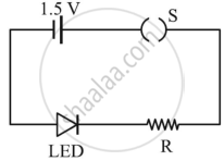
- A student connects the blue coloured LED as shown in the figure. The LED did not glow when switch S is closed. Explain why?

OR
iii. Draw V-I characteristic of a p-n junction diode in
(i) forward bias and (ii) reverse bias
Draw solar cells of I-V characteristics.
Draw the circuit diagram of an illuminated photodiode and its I-V characteristics.

