Advertisements
Advertisements
Question
The plate resistance of a triode is 8 kΩ and the transconductance is 2.5 millimho. (a) If the plate voltage is increased by 48 V and the grid voltage is kept constant, what will be the increase in the plate current? (b) With plate voltage kept constant at this increased value, by how much should the grid voltage be decreased in order to bring the plate current back to its initial value?
Solution
Given:-
Plate resistance,
`r_p=8KOmega=8000kOmega`
Change in plate voltage,
`deltaV_p=48V`
Formula for plate resistance:
\[r_P = \left( \frac{\delta V_P}{\delta I_P} \right)_{V_G = \text{constant}} \]
\[ \Rightarrow \delta I_p = \frac{\delta V_p}{r_p} {}_{V_{G = \text{constant}}} \]
\[ \Rightarrow \delta I_p = \frac{48}{8000} = 0 . 006 A = 6 \text{ mA}\]
(b) Now, Vp is kept constant.
Change in plate current,
`deltaI_p=6"mA"=0.006A`
Trasconductance,
\[g_m = 0 . 0025 mho\]
\[\delta V_G = \frac{\delta I_p}{g_m} = \frac{0 . 006}{0 . 0025}\]
\[\delta V_G = 2 . 4 V, \text{ at constant plate voltage}\]
APPEARS IN
RELATED QUESTIONS
Explain with the help of a diagram, how depletion region and potential barrier are formed in a junction diode.
Using the necessary circuit diagrams, show how the V-I characteristics of a p-n junction are obtained in
Forward biasing
How are these characteristics made use of in rectification?
State its any ‘two’ uses of photodiode.
Describe, with the help of a circuit diagram, the working of a photodiode.
Write briefly the important processes that occur during the formation of p−n junction. With the help of necessary diagrams, explain the term 'barrier potential'.
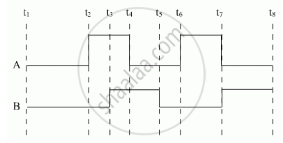
Show the output waveforms (Y) for the following inputs A and B of (i) OR gate (ii) NAND gate ?

Draw the circuit diagram of an illuminated photodiode in reverse bias. How is photodiode used to measure light intensity?
Explain the formation of depletion layer and potential barrier in a p−n junction.
Write the important considerations which are to be taken into account while fabricating a p-n junction diode to be used as a Light Emitting Diode (LED). What should be the order of the band gap of an LED, if it is required to emit light in the visible range? Draw a circuit diagram and explain its action.
Answer the following question.
Explain the three processes involved in solar cell working.
Pressure P varies as P = `alpha/beta "exp" (- (alpha x)/"k"_"BT")`, where x denotes the distance, kB is the Boltzmann's constant, T is the absolute temperature and α and β are constant. The dimension of β is ______.
A p-n photodiode is fabricated from a semiconductor with a band gap of 2.5 eV. lt can detect a signal of wavelength ______.
For LED's to emit light in visible region of electromagnetic light, it should have energy band gap in the range of:
In Figure, assuming the diodes to be ideal ______.

The amplifiers X, Y and Z are connected in series. If the voltage gains of X, Y and Z are 10, 20 and 30, respectively and the input signal is 1 mV peak value, then what is the output signal voltage (peak value)
- if dc supply voltage is 10V?
- if dc supply voltage is 5V?
Briefly explain how emf is generated in a solar cell.
