Advertisements
Advertisements
Question
Describe, with the help of a circuit diagram, the working of a photodiode.
Solution
Photo diode is a p-n junction diode made of photosensitive semiconductor in which current carriers are generated by photons through photo excitation, i.e., photo conduction by light. It is operated under reverse bias below the breakdown voltage.

Working of Photo diode
- The diode is fabricated such that the generation of e-h pairs takes place in or near the depletion region of the diode.
When visible light of energy greater than forbidden energy gap (
- These charge carriers will be separated by the junction and made to flow across the junction, creating a reverse current across the junction.
- The direction of the electric field is such that electrons reach n-side and holes are
- The value of reverse saturation current increases with the increase in the intensity of incident light as shown here. Hence, thereverse saturation current through the photo diode varies linearly with the light intensity.
- collected on p-side giving rise to an emf.
I – V characteristics of photo diode

APPEARS IN
RELATED QUESTIONS
How is a Zener diode fabricated?
Explain with the help of a diagram, how depletion region and potential barrier are formed in a junction diode.
Using the necessary circuit diagrams, show how the V-I characteristics of a p-n junction are obtained in
Reverse biasing
How are these characteristics made use of in rectification?
State its any ‘two’ uses of photodiode.
Write briefly the important processes that occur during the formation of p−n junction. With the help of necessary diagrams, explain the term 'barrier potential'.
Briefly explain its working. Draw its V - I characteristics for two different intensities of illumination ?
The current in the forward bias is known to be more (~mA) than the current in the reverse bias (~μA). What is the reason, then, to operate the photodiode in reverse bias?
For LED's to emit light in visible region of electromagnetic light, it should have energy band gap in the range of:
Read the following paragraph and answer the questions.
|
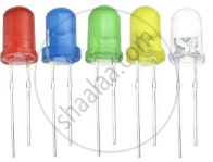
LED is a heavily doped P-N junction which under forward bias emits spontaneous radiation. When it is forward-biased, due to recombination of holes and electrons at the junction, energy is released in the form of photons. In the case of Si and Ge diode, the energy released in recombination lies in the infrared region. LEDs that can emit red, yellow, orange, green and blue light are commercially available. The semiconductor used for fabrication of visible LEDs must at least have a band gap of 1.8 eV. The compound semiconductor Gallium Arsenide – Phosphide is used for making LEDs of different colours.
|
- Why are LEDs made of compound semiconductor and not of elemental semiconductors?
- What should be the order of bandgap of an LED, if it is required to emit light in the visible range?
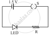
- A student connects the blue coloured LED as shown in the figure. The LED did not glow when switch S is closed. Explain why?
OR
iii. Draw V-I characteristic of a p-n junction diode in
(i) forward bias and (ii) reverse bias
How can a photodiode be used to measure light intensity?
