Advertisements
Advertisements
Question
Using the necessary circuit diagrams, show how the V-I characteristics of a p-n junction are obtained in
Reverse biasing
How are these characteristics made use of in rectification?
Solution
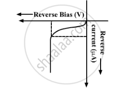
p-n junction diode under reverse bias

Positive terminal of battery is connected to n-side and negative terminal to p-side.
Reverse bias supports the potential barrier. Therefore, the barrier height increases and the width of depletion region also increases.
Due to the majority carriers, there is no conduction across the junction. A few minority carriers cross the junction after being accelerated by high reverse bias voltage.
This constitutes a current that flows in opposite direction, which is called reverse current.
The V-I characteristics of p-n junction diode in reverse bias is shown below:

p-n junction diode is used as a half-wave rectifier. Its working is based on the fact that the resistance of p-n junction becomes low when forward biased and becomes high when reverse biased. These characteristics of diode is used in rectification.
APPEARS IN
RELATED QUESTIONS
With the help of a neat circuit diagram, explain the working of a photodiode.
How is a Zener diode fabricated?
Why is zener diode fabricated by heavily doping both p- and n-sides of the junction?
Briefly explain its working. Draw its V - I characteristics for two different intensities of illumination ?
Draw V − I characteristics of a p-n junction diode. Answer the following questions, giving reasons:
(i) Why is the current under reverse bias almost independent of the applied potential up to a critical voltage?
(ii) Why does the reverse current show a sudden increase at the critical voltage?
Name any semiconductor device which operates under the reverse bias in the breakdown region.
Draw the circuit diagram of an illuminated photodiode in reverse bias. How is photodiode used to measure light intensity?
Choose the correct answer from given options
The wavelength and intensity of light emitted by a LED depend upon
Answer the following question.
Draw solar cell V-I characteristics.
Consider the following statements (A) and (B) and identify the correct answer.
- A Zener diode is connected in reverse bias when used as a voltage regulator.
- The potential barrier of the p-n junction lies between 0.1 V to 0.3 V.
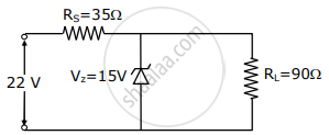
The value of power dissipated across the Zener diode (Vz = 15 V) connected in the circuit as shown in the figure is x × 10–1 watt. The value of x, to the nearest integer, is ______.

