Advertisements
Advertisements
Question
Why is zener diode fabricated by heavily doping both p- and n-sides of the junction?
Solution
A zener diode is fabricated by heavily doping both p- and n-sides of the junction so that its depletion region formed is very thin and the electric field of the junction is extremely high, even for a small reverse bias voltage.
RELATED QUESTIONS
How is a Zener diode fabricated?
With what considerations in view, a photodiode is fabricated? State its working with the help of a suitable diagram.
Even though the current in the forward bias is known to be more than in the reverse bias, yet the photodiode works in reverse bias. What is the reason?
Write briefly the important processes that occur during the formation of p−n junction. With the help of necessary diagrams, explain the term 'barrier potential'.
Choose the correct answer from given options
The wavelength and intensity of light emitted by a LED depend upon
What is a solar cell?
Answer the following question.
Draw solar cell V-I characteristics.
A p-n photodiode is fabricated from a semiconductor with a band gap of 2.5 eV. lt can detect a signal of wavelength ______.
Draw the circuit diagram of an illuminated photodiode and its I-V characteristics.
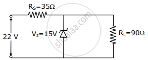
The value of power dissipated across the Zener diode (Vz = 15 V) connected in the circuit as shown in the figure is x × 10–1 watt. The value of x, to the nearest integer, is ______.

What energy conversion takes place in a solar cell?
