Advertisements
Advertisements
प्रश्न
Why is zener diode fabricated by heavily doping both p- and n-sides of the junction?
उत्तर
A zener diode is fabricated by heavily doping both p- and n-sides of the junction so that its depletion region formed is very thin and the electric field of the junction is extremely high, even for a small reverse bias voltage.
संबंधित प्रश्न
Explain with the help of a diagram, how depletion region and potential barrier are formed in a junction diode.
Using the necessary circuit diagrams, show how the V-I characteristics of a p-n junction are obtained in
Forward biasing
How are these characteristics made use of in rectification?
A p-n photodiode is fabricated from a semiconductor with band gap of 2.8 eV. Can it detect a wavelength of 6000 nm?
Describe, with the help of a circuit diagram, the working of a photodiode.
Draw V − I characteristics of a p-n junction diode. Answer the following questions, giving reasons:
(i) Why is the current under reverse bias almost independent of the applied potential up to a critical voltage?
(ii) Why does the reverse current show a sudden increase at the critical voltage?
Name any semiconductor device which operates under the reverse bias in the breakdown region.
What happens to the width of depletion player of a p-n junction when it is (i) forward biased, (ii) reverse biased?
An ideal diode should pass a current freely in one direction and should stop it completely in the opposite direction. Which is closer to ideal-vacuum diode or a p-njunction diode?
Choose the correct answer from given options
The wavelength and intensity of light emitted by a LED depend upon
Pressure P varies as P = `alpha/beta "exp" (- (alpha x)/"k"_"BT")`, where x denotes the distance, kB is the Boltzmann's constant, T is the absolute temperature and α and β are constant. The dimension of β is ______.
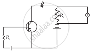
If the resistance R1 is increased (Figure), how will the readings of the ammeter and voltmeter change?

