Advertisements
Advertisements
Question
A p-n photodiode is fabricated from a semiconductor with band gap of 2.8 eV. Can it detect a wavelength of 6000 nm?
Solution
Energy band gap of the given photodiode, Eg = 2.8 eV
Wavelength, λ = 6000 nm = 6000 × 10−9 m
The energy of a signal is given by the relation:
`"E" = ("hc")/lambda`
Where
h = Planck’s constant
= 6.626 × 10⁻³⁴ Js
c = Speed of light
= 3 × 10⁸ m/s
`"E" = (6.626 xx 10^(-34) xx 3 xx 10^8)/(6000 xx 10^(-9))`
= 3.313 × 10⁻²⁰ J
But 1.6 × 10⁻¹⁹ J = 1 eV
∴ E = 3.313 × 10⁻²⁰ J
`= (3.313 xx 10^(-20))/(1.6 xx 10^(-19)) = 0.207 " eV"`
The energy of a signal of wavelength 6000 nm is 0.207 eV, which is less than 2.8 eV − the energy band gap of a photodiode. Hence, the photodiode cannot detect the signal.
APPEARS IN
RELATED QUESTIONS
With the help of a neat circuit diagram, explain the working of a photodiode.
How is a Zener diode fabricated?
If a small voltage is applied to a p-n junction diode, how will the barrier potential be affected when it is (i) forward biased
Using the necessary circuit diagrams, show how the V-I characteristics of a p-n junction are obtained in
Reverse biasing
How are these characteristics made use of in rectification?
Sunil and his parents were travelling to their village in their car. On the way his mother noticed some grey coloured panels installed on the roof of a low building. She enquired from Sunil what those panels were and Sunil told his mother that those were solar panels.
(a) What were the values displayed by Sunil and his mother? State one value for each.
(b) In what way would the use of solar panels prove to be very useful?
(c) Name the semiconductor device used in solar panels. Briefly explain with the help of a diagram, how this device works
Write briefly the important processes that occur during the formation of p−n junction. With the help of necessary diagrams, explain the term 'barrier potential'.
Briefly explain its working. Draw its V - I characteristics for two different intensities of illumination ?
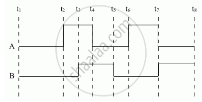
Show the output waveforms (Y) for the following inputs A and B of (i) OR gate (ii) NAND gate ?
How does a light emitting diode (LED) work? Give two advantages of LED’s over the conventional incandescent lamps.
The plate resistance of a triode is 8 kΩ and the transconductance is 2.5 millimho. (a) If the plate voltage is increased by 48 V and the grid voltage is kept constant, what will be the increase in the plate current? (b) With plate voltage kept constant at this increased value, by how much should the grid voltage be decreased in order to bring the plate current back to its initial value?
Write the important considerations which are to be taken into account while fabricating a p-n junction diode to be used as a Light Emitting Diode (LED). What should be the order of the band gap of an LED, if it is required to emit light in the visible range? Draw a circuit diagram and explain its action.
What is a solar cell?
Explain photodiode.
A p-n photodiode is fabricated from a semiconductor with a band gap of 2.5 eV. lt can detect a signal of wavelength ______.
For LED's to emit light in visible region of electromagnetic light, it should have energy band gap in the range of:
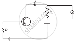
If the resistance R1 is increased (Figure), how will the readings of the ammeter and voltmeter change?
Read the following paragraph and answer the questions.
|
LED is a heavily doped P-N junction which under forward bias emits spontaneous radiation. When it is forward-biased, due to recombination of holes and electrons at the junction, energy is released in the form of photons. In the case of Si and Ge diode, the energy released in recombination lies in the infrared region. LEDs that can emit red, yellow, orange, green and blue light are commercially available. The semiconductor used for fabrication of visible LEDs must at least have a band gap of 1.8 eV. The compound semiconductor Gallium Arsenide – Phosphide is used for making LEDs of different colours.
|
- Why are LEDs made of compound semiconductor and not of elemental semiconductors?
- What should be the order of bandgap of an LED, if it is required to emit light in the visible range?
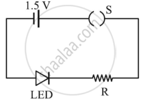
- A student connects the blue coloured LED as shown in the figure. The LED did not glow when switch S is closed. Explain why?
OR
iii. Draw V-I characteristic of a p-n junction diode in
(i) forward bias and (ii) reverse bias
Why a photo-diode is operated in reverse bias whereas the current in the forward bias is much larger than that in the reverse bias? Explain. Mention its two uses.
