Advertisements
Advertisements
प्रश्न
A p-n photodiode is fabricated from a semiconductor with band gap of 2.8 eV. Can it detect a wavelength of 6000 nm?
उत्तर
Energy band gap of the given photodiode, Eg = 2.8 eV
Wavelength, λ = 6000 nm = 6000 × 10−9 m
The energy of a signal is given by the relation:
`"E" = ("hc")/lambda`
Where
h = Planck’s constant
= 6.626 × 10⁻³⁴ Js
c = Speed of light
= 3 × 10⁸ m/s
`"E" = (6.626 xx 10^(-34) xx 3 xx 10^8)/(6000 xx 10^(-9))`
= 3.313 × 10⁻²⁰ J
But 1.6 × 10⁻¹⁹ J = 1 eV
∴ E = 3.313 × 10⁻²⁰ J
`= (3.313 xx 10^(-20))/(1.6 xx 10^(-19)) = 0.207 " eV"`
The energy of a signal of wavelength 6000 nm is 0.207 eV, which is less than 2.8 eV − the energy band gap of a photodiode. Hence, the photodiode cannot detect the signal.
APPEARS IN
संबंधित प्रश्न
Colour of light emitted by LED depends upon__________________ .
- its forward bias
- its reverse bias
- the band gap of the material of semiconductor
- its size
How is a Zener diode fabricated?
If a small voltage is applied to a p-n junction diode, how will the barrier potential be affected when it is(ii) reveres biased?
Carbon, silicon and germanium have four valence electrons each. These are characterised by valence and conduction bands separated by energy band gap respectively equal to (Eg)C, (Eg)Si and (Eg)Ge. Which of the following statements is true?
The width of depletion region of p-n junction diode is _______.
(A) 0.5 nm to 1 nm
(B) 5 nm to 10 nm
(C) 50 nm to 500 nm
(D) 500 nm to 1000 nm
Why is zener diode fabricated by heavily doping both p- and n-sides of the junction?
Briefly explain its working. Draw its V - I characteristics for two different intensities of illumination ?
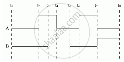
Show the output waveforms (Y) for the following inputs A and B of (i) OR gate (ii) NAND gate ?

Draw the circuit diagram of an illuminated photodiode in reverse bias. How is photodiode used to measure light intensity?
An ideal diode should pass a current freely in one direction and should stop it completely in the opposite direction. Which is closer to ideal-vacuum diode or a p-njunction diode?
Draw the circuit arrangement for studying the V-I characteristics of a p-n junction diode in reverse bias. Plot the V-I characteristics in this case.
With reference to Semiconductor Physics,
Name the process that causes depletion region in a p-n junction.
Pressure P varies as P = `alpha/beta "exp" (- (alpha x)/"k"_"BT")`, where x denotes the distance, kB is the Boltzmann's constant, T is the absolute temperature and α and β are constant. The dimension of β is ______.
A p-n photodiode is fabricated from a semiconductor with a band gap of 2.5 eV. lt can detect a signal of wavelength ______.
Which one of the following is not the advantage of LED?
Consider the following statements (A) and (B) and identify the correct answer.
- A Zener diode is connected in reverse bias when used as a voltage regulator.
- The potential barrier of the p-n junction lies between 0.1 V to 0.3 V.
In Figure, assuming the diodes to be ideal ______.

Why a photo-diode is operated in reverse bias whereas the current in the forward bias is much larger than that in the reverse bias? Explain. Mention its two uses.
Briefly explain how emf is generated in a solar cell.
