Advertisements
Advertisements
प्रश्न
An ideal diode should pass a current freely in one direction and should stop it completely in the opposite direction. Which is closer to ideal-vacuum diode or a p-njunction diode?
उत्तर
It should be an ideal vacuum diode. When a pn junction diode is reverse biassed then a small current called reverse current flows across the diode.As the the p‒n junction diode allows some current in reverse biassed condition also so the given diode can not be a pn junction diode.
APPEARS IN
संबंधित प्रश्न
Meeta's father was driving her to school. At the traffic signal, she noticed that each traffic light was made of many tiny lights instead of a single bulb. When Meeta asked this question to her father, he explained the reason for this.
Answer the following questions based on above information:
(i) What were the values displayed by Meeta and her father?
(ii) What answer did Meeta's father give?
(iii) What are the tiny lights in traffic signals called and how do these operate?
Carbon, silicon and germanium have four valence electrons each. These are characterised by valence and conduction bands separated by energy band gap respectively equal to (Eg)C, (Eg)Si and (Eg)Ge. Which of the following statements is true?
The width of depletion region of p-n junction diode is _______.
(A) 0.5 nm to 1 nm
(B) 5 nm to 10 nm
(C) 50 nm to 500 nm
(D) 500 nm to 1000 nm
Describe, with the help of a circuit diagram, the working of a photodiode.
Why is zener diode fabricated by heavily doping both p- and n-sides of the junction?
How is a photodiode fabricated?
Briefly explain its working. Draw its V - I characteristics for two different intensities of illumination ?
Draw V − I characteristics of a p-n junction diode. Answer the following questions, giving reasons:
(i) Why is the current under reverse bias almost independent of the applied potential up to a critical voltage?
(ii) Why does the reverse current show a sudden increase at the critical voltage?
Name any semiconductor device which operates under the reverse bias in the breakdown region.
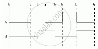
Show the output waveforms (Y) for the following inputs A and B of (i) OR gate (ii) NAND gate ?

How does a light emitting diode (LED) work? Give two advantages of LED’s over the conventional incandescent lamps.
What happens to the width of depletion player of a p-n junction when it is (i) forward biased, (ii) reverse biased?
Explain the formation of depletion layer and potential barrier in a p−n junction.
Draw the V-I characteristics of an LED. State two advantages of LED lamps over convertional incandescent lamps.
Choose the correct answer from given options
The wavelength and intensity of light emitted by a LED depend upon
Explain photodiode.
For LED's to emit light in visible region of electromagnetic light, it should have energy band gap in the range of:
In Figure, assuming the diodes to be ideal ______.

Draw solar cells of I-V characteristics.
