Advertisements
Advertisements
प्रश्न
Carbon, silicon and germanium have four valence electrons each. These are characterised by valence and conduction bands separated by energy band gap respectively equal to (Eg)C, (Eg)Si and (Eg)Ge. Which of the following statements is true?
विकल्प
(Eg)Si < (Eg)Ge < (Eg)C
(Eg)C < (Eg)Ge > (Eg)Si
(Eg)C > (Eg)Si > (Eg)Ge
(Eg)C = (Eg)Si = (Eg)Ge
उत्तर
(Eg)C > (Eg)Si > (Eg)Ge
Explanation:
Of the three given elements, the energy band gap of carbon is the maximum and that of germanium is the least.
The energy band gap of these elements are related as: (Eg)C > (Eg)Si > (Eg)Ge
APPEARS IN
संबंधित प्रश्न
Colour of light emitted by LED depends upon__________________ .
- its forward bias
- its reverse bias
- the band gap of the material of semiconductor
- its size
Meeta's father was driving her to school. At the traffic signal, she noticed that each traffic light was made of many tiny lights instead of a single bulb. When Meeta asked this question to her father, he explained the reason for this.
Answer the following questions based on above information:
(i) What were the values displayed by Meeta and her father?
(ii) What answer did Meeta's father give?
(iii) What are the tiny lights in traffic signals called and how do these operate?
Using the necessary circuit diagrams, show how the V-I characteristics of a p-n junction are obtained in
Forward biasing
How are these characteristics made use of in rectification?
Write briefly the important processes that occur during the formation of p−n junction. With the help of necessary diagrams, explain the term 'barrier potential'.
Draw V − I characteristics of a p-n junction diode. Answer the following questions, giving reasons:
(i) Why is the current under reverse bias almost independent of the applied potential up to a critical voltage?
(ii) Why does the reverse current show a sudden increase at the critical voltage?
Name any semiconductor device which operates under the reverse bias in the breakdown region.
Draw the circuit diagram of a full wave rectifier using p-n junction diode.
Explain its working and show the output, input waveforms.
Draw the circuit diagram of an illuminated photodiode in reverse bias. How is photodiode used to measure light intensity?
Explain the formation of depletion layer and potential barrier in a p−n junction.
Write the important considerations which are to be taken into account while fabricating a p-n junction diode to be used as a Light Emitting Diode (LED). What should be the order of the band gap of an LED, if it is required to emit light in the visible range? Draw a circuit diagram and explain its action.
Choose the correct answer from given options
The wavelength and intensity of light emitted by a LED depend upon
Answer the following question.
Draw solar cell V-I characteristics.
With reference to Semiconductor Physics,
Name the process that causes depletion region in a p-n junction.
Pressure P varies as P = `alpha/beta "exp" (- (alpha x)/"k"_"BT")`, where x denotes the distance, kB is the Boltzmann's constant, T is the absolute temperature and α and β are constant. The dimension of β is ______.
For LED's to emit light in visible region of electromagnetic light, it should have energy band gap in the range of:
Which one of the following is not the advantage of LED?
Read the following paragraph and answer the questions.
|
LED is a heavily doped P-N junction which under forward bias emits spontaneous radiation. When it is forward-biased, due to recombination of holes and electrons at the junction, energy is released in the form of photons. In the case of Si and Ge diode, the energy released in recombination lies in the infrared region. LEDs that can emit red, yellow, orange, green and blue light are commercially available. The semiconductor used for fabrication of visible LEDs must at least have a band gap of 1.8 eV. The compound semiconductor Gallium Arsenide – Phosphide is used for making LEDs of different colours.
|
- Why are LEDs made of compound semiconductor and not of elemental semiconductors?
- What should be the order of bandgap of an LED, if it is required to emit light in the visible range?
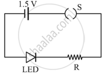
- A student connects the blue coloured LED as shown in the figure. The LED did not glow when switch S is closed. Explain why?
OR
iii. Draw V-I characteristic of a p-n junction diode in
(i) forward bias and (ii) reverse bias
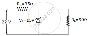
The value of power dissipated across the Zener diode (Vz = 15 V) connected in the circuit as shown in the figure is x × 10–1 watt. The value of x, to the nearest integer, is ______.