Advertisements
Online Mock Tests
Chapters
2: Electrostatic Potential and Capacitance
3: Current Electricity
4: Moving Charges and Magnetism
5: Magnetism and Matter
6: Electromagnetic Induction
7: Alternating Current
8: Electromagnetic Waves
9: Ray Optics and Optical Instruments
10: Wave Optics
11: Dual Nature of Radiation and Matter
12: Atoms
13: Nuclei
▶ 14: Semiconductor Electronics: Materials, Devices and Simple Circuits
15: Communication Systems
![NCERT solutions for Physics [English] Class 12 chapter 14 - Semiconductor Electronics: Materials, Devices and Simple Circuits - Shaalaa.com](/images/9788174506313-physics-english-class-12_6:cdb96651cad74f93ac9629abf3654ecd.jpg "NCERT solutions for Physics [English] Class 12 chapter 14 - Semiconductor Electronics: Materials, Devices and Simple Circuits")
Advertisements
Solutions for Chapter 14: Semiconductor Electronics: Materials, Devices and Simple Circuits
Below listed, you can find solutions for Chapter 14 of CBSE, Karnataka Board PUC NCERT for Physics [English] Class 12.
NCERT solutions for Physics [English] Class 12 14 Semiconductor Electronics: Materials, Devices and Simple Circuits Exercise [Pages 509 - 512]
In an n-type silicon, which of the following statement is true:
Electrons are majority carriers and trivalent atoms are the dopants.
Electrons are minority carriers and pentavalent atoms are the dopants.
Holes are minority carriers and pentavalent atoms are the dopants.
Holes are majority carriers and trivalent atoms are the dopants.
In a p-type semiconductos, which of the following statement is true:
Electrons are majority carriers and trivalent atoms are the dopants.
Electrons are minority carriers and pentavalent atoms are the dopants.
Holes are minority carriers and pentavalent atoms are the dopants.
Holes are majority carriers and trivalent atoms are the dopants.
Carbon, silicon and germanium have four valence electrons each. These are characterised by valence and conduction bands separated by energy band gap respectively equal to (Eg)C, (Eg)Si and (Eg)Ge. Which of the following statements is true?
(Eg)Si < (Eg)Ge < (Eg)C
(Eg)C < (Eg)Ge > (Eg)Si
(Eg)C > (Eg)Si > (Eg)Ge
(Eg)C = (Eg)Si = (Eg)Ge
In an unbiased p-n junction, holes diffuse from the p-region to n-region because ______.
free electrons in the n-region attract them.
they move across the junction by the potential difference.
hole concentration in p-region is more as compared to n-region.
All the above.
When a forward bias is applied to a p-n junction, it ______.
raises the potential barrier.
reduces the majority carrier current to zero.
lowers the potential barrier.
None of the above.
For transistor action, which of the following statements are correct:
(a) Base, emitter and collector regions should have similar size and doping concentrations.
(b) The base region must be very thin and lightly doped.
(c) The emitter junction is forward biased and collector junction is reverse biased.
(d) Both the emitter junction as well as the collector junction are forward biased.
For a transistor amplifier, the voltage gain
(a) remains constant for all frequencies.
(b) is high at high and low frequencies and constant in the middle frequency range.
(c) is low at high and low frequencies and constant at mid frequencies.
(d) None of the above.
In half-wave rectification, what is the output frequency if the input frequency is 50 Hz. What is the output frequency of a full-wave rectifier for the same input frequency.
For a CE-transistor amplifier, the audio signal voltage across the collector resistance of 2 kΩ is 2 V. Suppose the current amplification factor of the transistor is 100, find the input signal voltage and base current if the base resistance is 1 kΩ.
Two amplifiers are connected one after the other in series (cascaded). The first amplifier has a voltage gain of 10 and the second has a voltage gain of 20. If the input signal is 0.01 volt, calculate the output ac signal.
A p-n photodiode is fabricated from a semiconductor with band gap of 2.8 eV. Can it detect a wavelength of 6000 nm?
The number of silicon atoms per m3 is 5 × 1028. This is doped simultaneously with 5 × 10²² atoms per m3 of Arsenic and 5 × 10²⁰ per m3 atoms of Indium. Calculate the number of electrons and holes. Given that ni= 1.5 × 10¹⁶ m−3. Is the material n-type or p-type?
In an intrinsic semiconductor the energy gap Egis 1.2 eV. Its hole mobility is much smaller than electron mobility and independent of temperature. What is the ratio between conductivity at 600K and that at 300K? Assume that the temperature dependence of intrinsic carrier concentration niis given by
`"n"_"i" = "n"_0 exp(- "E"_"g"/(2"k"_"BT"))`
where n0 is a constant.
In a p-n junction diode, the current I can be expressed as
I = `"I"_0 exp ("eV"/(2"k"_"BT") - 1)`
where I0 is called the reverse saturation current, V is the voltage across the diode and is positive for forward bias and negative for reverse bias, and I is the current through the diode, kBis the Boltzmann constant (8.6×10⁻⁵ eV/K) and T is the absolute temperature. If for a given diode I0 = 5 × 10⁻¹² A and T = 300 K, then
(a) What will be the forward current at a forward voltage of 0.6 V?
(b) What will be the increase in the current if the voltage across the diode is increased to 0.7 V?
(c) What is the dynamic resistance?
(d) What will be the current if reverse bias voltage changes from 1 V to 2 V?
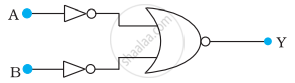
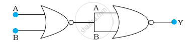
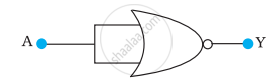
You are given the two circuits as shown in following figure. Show that circuit
- acts as OR gate while the circuit
- acts as AND gate.
(a)
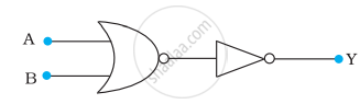
(b)
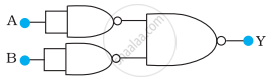
Write the truth table for a NAND gate connected as given in the following figure.
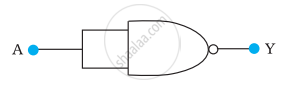
Hence identify the exact logic operation carried out by this circuit
You are given two circuits as shown in following figure, which consist of NAND gates. Identify the logic operation carried out by the two circuits.
(a)
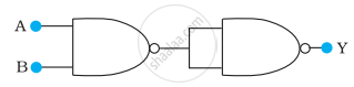
(b)
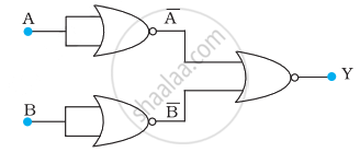
Write the truth table for circuit given in figure below consisting of NOR gates and identify the logic operation (OR, AND, NOT) which this circuit is performing.
(Hint: A = 0, B = 1 then A and B inputs of second NOR gate will be 0 and hence Y=1. Similarly work out the values of Y for other combinations of A and B. Compare with the truth table of OR, AND, NOT gates and find the correct one.)
Write the truth table for the circuits given in following figure consisting of NOR gates only. Identify the logic operations (OR, AND, NOT) performed by the two circuits.
(a)
(b)
Solutions for 14: Semiconductor Electronics: Materials, Devices and Simple Circuits
NCERT solutions for Physics [English] Class 12 chapter 14 - Semiconductor Electronics: Materials, Devices and Simple Circuits
Shaalaa.com has the CBSE, Karnataka Board PUC Mathematics Physics [English] Class 12 CBSE, Karnataka Board PUC solutions in a manner that help students grasp basic concepts better and faster. The detailed, step-by-step solutions will help you understand the concepts better and clarify any confusion. NCERT solutions for Mathematics Physics [English] Class 12 CBSE, Karnataka Board PUC 14 (Semiconductor Electronics: Materials, Devices and Simple Circuits) include all questions with answers and detailed explanations. This will clear students' doubts about questions and improve their application skills while preparing for board exams.
Further, we at Shaalaa.com provide such solutions so students can prepare for written exams. NCERT textbook solutions can be a core help for self-study and provide excellent self-help guidance for students.
Concepts covered in Physics [English] Class 12 chapter 14 Semiconductor Electronics: Materials, Devices and Simple Circuits are Concept of Semiconductor Electronics: Materials, Devices and Simple Circuits, Integrated Circuits, Feedback Amplifier and Transistor Oscillator, Transistor as a Device, Basic Transistor Circuit Configurations and Transistor Characteristics, Application of Junction Diode as a Rectifier, p-n Junction, Intrinsic Semiconductor, Classification of Metals, Conductors and Semiconductors, Extrinsic Semiconductor, Transistor Action, Transistor: Structure and Action, Semiconductor Diode, Energy Bands in Conductors, Semiconductors and Insulators, Triode, Digital Electronics and Logic Gates, Transistor as an Amplifier (Ce-configuration), Transistor and Characteristics of a Transistor, Zener Diode as a Voltage Regulator, Special Purpose P-n Junction Diodes, Diode as a Rectifier, Concept of Semiconductor Electronics: Materials, Devices and Simple Circuits, Integrated Circuits, Feedback Amplifier and Transistor Oscillator, Transistor as a Device, Basic Transistor Circuit Configurations and Transistor Characteristics, Application of Junction Diode as a Rectifier, p-n Junction, Intrinsic Semiconductor, Classification of Metals, Conductors and Semiconductors, Extrinsic Semiconductor, Transistor Action, Transistor: Structure and Action, Semiconductor Diode, Energy Bands in Conductors, Semiconductors and Insulators, Triode, Digital Electronics and Logic Gates, Transistor as an Amplifier (Ce-configuration), Transistor and Characteristics of a Transistor, Zener Diode as a Voltage Regulator, Special Purpose P-n Junction Diodes, Diode as a Rectifier.
Using NCERT Physics [English] Class 12 solutions Semiconductor Electronics: Materials, Devices and Simple Circuits exercise by students is an easy way to prepare for the exams, as they involve solutions arranged chapter-wise and also page-wise. The questions involved in NCERT Solutions are essential questions that can be asked in the final exam. Maximum CBSE, Karnataka Board PUC Physics [English] Class 12 students prefer NCERT Textbook Solutions to score more in exams.
Get the free view of Chapter 14, Semiconductor Electronics: Materials, Devices and Simple Circuits Physics [English] Class 12 additional questions for Mathematics Physics [English] Class 12 CBSE, Karnataka Board PUC, and you can use Shaalaa.com to keep it handy for your exam preparation.
