Advertisements
Advertisements
प्रश्न
Draw V − I characteristics of a p-n junction diode. Answer the following questions, giving reasons:
(i) Why is the current under reverse bias almost independent of the applied potential up to a critical voltage?
(ii) Why does the reverse current show a sudden increase at the critical voltage?
Name any semiconductor device which operates under the reverse bias in the breakdown region.
उत्तर
V-I characteristic of p-n junction diode:
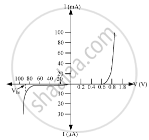
(i) Under the reverse bias condition, the holes of p-side are attracted towards the negative terminal of the battery and the electrons of the n-side are attracted towards the positive terminal of the battery. This increases the depletion layer and the potential barrier. However the minority charge carriers are drifted across the junction producing a small current. At any temperature the number of minority carriers is constant so there is the small current at any applied potential. This is the reason for the current under reverse bias to be almost independent of applied potential. At the critical voltage, avalanche breakdown takes place which results in a sudden flow of large current.
(ii) At the critical voltage, the holes in the n-side and conduction electrons in the p-side are accelerated due to the reverse −bias voltage. These minority carriers acquire sufficient kinetic energy from the electric field and collide with a valence electron. Thus the bond is finally broken and the valence electrons move into the conduction band resulting in enormous flow of electrons and thus formation of hole-electron pairs. Thus there is a sudden increase in the current at the critical voltage.
Zener diode is a semiconductor device which operates under the reverse bias in the breakdown region.
APPEARS IN
संबंधित प्रश्न
Carbon, silicon and germanium have four valence electrons each. These are characterised by valence and conduction bands separated by energy band gap respectively equal to (Eg)C, (Eg)Si and (Eg)Ge. Which of the following statements is true?
Describe, with the help of a circuit diagram, the working of a photodiode.
Write briefly the important processes that occur during the formation of p−n junction. With the help of necessary diagrams, explain the term 'barrier potential'.
Why is zener diode fabricated by heavily doping both p- and n-sides of the junction?
How is a photodiode fabricated?
What happens to the width of depletion player of a p-n junction when it is (i) forward biased, (ii) reverse biased?
Explain how a potential barrier is developed in a p-n junction diode.
Draw the V-I characteristics of an LED. State two advantages of LED lamps over convertional incandescent lamps.
Write the important considerations which are to be taken into account while fabricating a p-n junction diode to be used as a Light Emitting Diode (LED). What should be the order of the band gap of an LED, if it is required to emit light in the visible range? Draw a circuit diagram and explain its action.
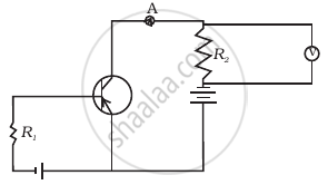
If the resistance R1 is increased (Figure), how will the readings of the ammeter and voltmeter change?