Advertisements
Advertisements
प्रश्न
Explain how a potential barrier is developed in a p-n junction diode.
उत्तर १
During the formation of p-n junction, and due to the concentration gradient across p-, and n- sides, holes
diffuse from p-side to n-side (p → n) and electrons diffuse from n-side to p-side (n → p). This motion of charge carries gives rise to diffusion current across the junction. When an electron diffuses from n → p, it leaves behind an ionised donor on n-side. This ionised donor (positive charge) is immobile as it is bonded to the surrounding atoms. As the electrons continue to diffuse from n → p, a layer of positive charge (or positive space-charge region) on n-side of the junction is developed.
उत्तर २
In a p-n junction diode, holes are the majority carriers on the p side whereas electrons are the majority carriers on the n-side of the semiconductor. Due to the diffusion of majority carriers from p-region to n-region, the p-region becomes less positive and n-region becomes less negative. An imaginary voltage is developed across the junction which prevents further movement of majority carriers across the junction. The voltage so developed is known as the potential barrier.
संबंधित प्रश्न
If a small voltage is applied to a p-n junction diode, how will the barrier potential be affected when it is (i) forward biased
Using the necessary circuit diagrams, show how the V-I characteristics of a p-n junction are obtained in
Reverse biasing
How are these characteristics made use of in rectification?
Sunil and his parents were travelling to their village in their car. On the way his mother noticed some grey coloured panels installed on the roof of a low building. She enquired from Sunil what those panels were and Sunil told his mother that those were solar panels.
(a) What were the values displayed by Sunil and his mother? State one value for each.
(b) In what way would the use of solar panels prove to be very useful?
(c) Name the semiconductor device used in solar panels. Briefly explain with the help of a diagram, how this device works
Draw the circuit diagram of an illuminated photodiode in reverse bias. How is photodiode used to measure light intensity?
An ideal diode should pass a current freely in one direction and should stop it completely in the opposite direction. Which is closer to ideal-vacuum diode or a p-njunction diode?
Answer the following question.
Explain the three processes involved in solar cell working.
What is the magnitude of the potential barrier across a Ge p-n junction?
The amplifiers X, Y and Z are connected in series. If the voltage gains of X, Y and Z are 10, 20 and 30, respectively and the input signal is 1 mV peak value, then what is the output signal voltage (peak value)
- if dc supply voltage is 10V?
- if dc supply voltage is 5V?
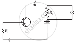
If the resistance R1 is increased (Figure), how will the readings of the ammeter and voltmeter change?

Briefly explain how emf is generated in a solar cell.
