Advertisements
Advertisements
प्रश्न
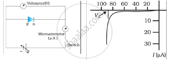
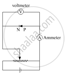
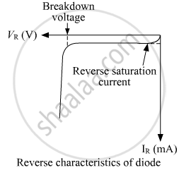
Draw the circuit arrangement for studying the V-I characteristics of a p-n junction diode in reverse bias. Plot the V-I characteristics in this case.
उत्तर १

उत्तर २
circuit arrangement for studying the V-I characteristics of a p-n junction diode in reverse bias:

V-I characteristics graph of a p-n junction diode in reverse bias:

संबंधित प्रश्न
Colour of light emitted by LED depends upon__________________ .
- its forward bias
- its reverse bias
- the band gap of the material of semiconductor
- its size
With what considerations in view, a photodiode is fabricated? State its working with the help of a suitable diagram.
Even though the current in the forward bias is known to be more than in the reverse bias, yet the photodiode works in reverse bias. What is the reason?
Sunil and his parents were travelling to their village in their car. On the way his mother noticed some grey coloured panels installed on the roof of a low building. She enquired from Sunil what those panels were and Sunil told his mother that those were solar panels.
(a) What were the values displayed by Sunil and his mother? State one value for each.
(b) In what way would the use of solar panels prove to be very useful?
(c) Name the semiconductor device used in solar panels. Briefly explain with the help of a diagram, how this device works
Briefly explain its working. Draw its V - I characteristics for two different intensities of illumination ?
Draw V − I characteristics of a p-n junction diode. Answer the following questions, giving reasons:
(i) Why is the current under reverse bias almost independent of the applied potential up to a critical voltage?
(ii) Why does the reverse current show a sudden increase at the critical voltage?
Name any semiconductor device which operates under the reverse bias in the breakdown region.
Draw the circuit diagram of a full wave rectifier using p-n junction diode.
Explain its working and show the output, input waveforms.
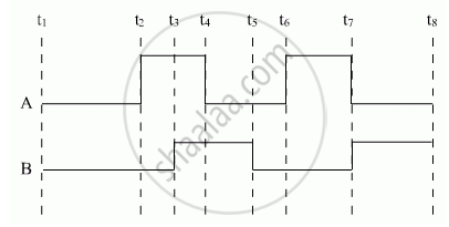
Show the output waveforms (Y) for the following inputs A and B of (i) OR gate (ii) NAND gate ?

Write the important considerations which are to be taken into account while fabricating a p-n junction diode to be used as a Light Emitting Diode (LED). What should be the order of band gap of an LED, if it is required to emit light in the visible range? Draw a circuit diagram and explain its action.
Pressure P varies as P = `alpha/beta "exp" (- (alpha x)/"k"_"BT")`, where x denotes the distance, kB is the Boltzmann's constant, T is the absolute temperature and α and β are constant. The dimension of β is ______.
For LED's to emit light in visible region of electromagnetic light, it should have energy band gap in the range of:
