Advertisements
Advertisements
प्रश्न
Explain the formation of depletion layer and potential barrier in a p−n junction.
उत्तर
In a p−n junction, a p-type and an n-type material are joined together. The concentration of holes is higher in p-type material as compared to that in n-type material. Therefore, there is a concentration gradient between the p-type and n-type materials. As a result of this concentration gradient, holes move from p-side to n-side (p → n) by the process of diffusion. Similarly, electrons move from n-side to p-side (n → p).
As the holes diffuse from p-side, they leave ionised spaces (negatively charged) on p-side near the junction. These ionised spaces are immobile. Hence, a negative space-charge region is formed on the p-side near the junction. Similarly, a positive space-charge region is formed on the n-side. These two space-charge regions on either sides of the junction constitute what is called a depletion layer.
Since the n-side loses electrons and p-side gains electrons, a potential difference is developed across the junction of the two regions. This potential difference tends to oppose further motions of electron from the n-region into the p-region. The same happens for holes too. The reverse polarity of this potential opposes further flow of carriers and is thus called the barrier potential.
APPEARS IN
संबंधित प्रश्न
Colour of light emitted by LED depends upon__________________ .
- its forward bias
- its reverse bias
- the band gap of the material of semiconductor
- its size
With what considerations in view, a photodiode is fabricated? State its working with the help of a suitable diagram.
Even though the current in the forward bias is known to be more than in the reverse bias, yet the photodiode works in reverse bias. What is the reason?
Carbon, silicon and germanium have four valence electrons each. These are characterised by valence and conduction bands separated by energy band gap respectively equal to (Eg)C, (Eg)Si and (Eg)Ge. Which of the following statements is true?
The width of depletion region of p-n junction diode is _______.
(A) 0.5 nm to 1 nm
(B) 5 nm to 10 nm
(C) 50 nm to 500 nm
(D) 500 nm to 1000 nm
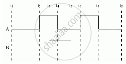
Show the output waveforms (Y) for the following inputs A and B of (i) OR gate (ii) NAND gate ?

What is a solar cell?
With reference to Semiconductor Physics,
Name the process that causes depletion region in a p-n junction.
Pressure P varies as P = `alpha/beta "exp" (- (alpha x)/"k"_"BT")`, where x denotes the distance, kB is the Boltzmann's constant, T is the absolute temperature and α and β are constant. The dimension of β is ______.
Consider the following statements (A) and (B) and identify the correct answer.
- A Zener diode is connected in reverse bias when used as a voltage regulator.
- The potential barrier of the p-n junction lies between 0.1 V to 0.3 V.
In Figure, assuming the diodes to be ideal ______.

