Advertisements
Advertisements
प्रश्न
How is a Zener diode fabricated?
Write two important considerations used while fabricating a Zener diode.
उत्तर १
A Zener diode is fabricated by heavily doping both p and n sides of the junction
उत्तर २
Two important considerations while fabricating a Zener diode are as follows:
(i) The Zener diode should be fabricated by heavily doping both p and n junctions.
(ii) Proper wafer-handling devices must be used to avoid contamination, which may affect the quality and stability of the diode.
APPEARS IN
संबंधित प्रश्न
With what considerations in view, a photodiode is fabricated? State its working with the help of a suitable diagram.
Even though the current in the forward bias is known to be more than in the reverse bias, yet the photodiode works in reverse bias. What is the reason?
The width of depletion region of p-n junction diode is _______.
(A) 0.5 nm to 1 nm
(B) 5 nm to 10 nm
(C) 50 nm to 500 nm
(D) 500 nm to 1000 nm
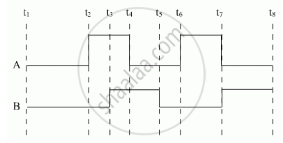
Show the output waveforms (Y) for the following inputs A and B of (i) OR gate (ii) NAND gate ?

Describe briefly, with the help of a diagram, the role of the two important processes involved in the formation of a p-n junction ?
An ideal diode should pass a current freely in one direction and should stop it completely in the opposite direction. Which is closer to ideal-vacuum diode or a p-njunction diode?
With reference to Semiconductor Physics,
Name the process that causes depletion region in a p-n junction.
Explain photodiode.
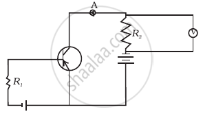
If the resistance R1 is increased (Figure), how will the readings of the ammeter and voltmeter change?

Draw solar cells of I-V characteristics.
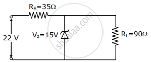
The value of power dissipated across the Zener diode (Vz = 15 V) connected in the circuit as shown in the figure is x × 10–1 watt. The value of x, to the nearest integer, is ______.

