Advertisements
Advertisements
Question
Explain the I-V characteristic of a forward-biased junction diode.
Solution
- Figure given below shows the I-V characteristic of a forward-biased diode.
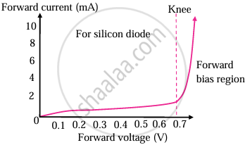
Forward biased characteristic of a diode - When connected in forward bias mode, initially, the current through the diode is very low and then there is a sudden rise in the current.
- The point at which currently rises sharply is shown as the ‘knee’ point on the I-V characteristic curve.
- The corresponding voltage is called the knee voltage. It is about 0.7 V for silicon and 0.3 V for germanium.
- A diode effectively becomes a short circuit above this knee point and can conduct a very large current.
- To limit the current flowing through the diode, resistors are used in series with the diode.
- If the current through a diode exceeds the specified value, the diode can heat up due to the Joule’s heating, and this may result in its physical damage.
APPEARS IN
RELATED QUESTIONS
Choose the correct option.
A reverse-biased diode is equivalent to:
Choose the correct option.
The potential barrier in p-n diode is due to:
Answer the following question.
What causes a larger current through a p-n junction diode when forward biased?
Answer in detail.
Explain the importance of the depletion region in a p-n junction diode.
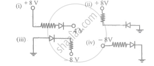
In the following figures, the diodes are either forward biased or reversed biased. Choose the CORRECT statement:
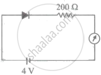
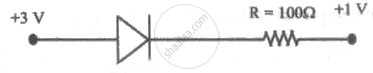
The reading of the ammeter for a silicon diode in the given circuit is:
In case of p-n junction diode, the width of depletion region is ______.
Consider the junction diode as ideal. The value of current flowing through AB is ______.
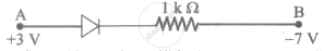
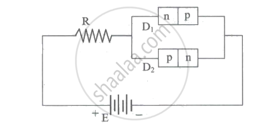
Figure shows two p-n junction diodes along with a resistance R and a dc battery E. The path of flow of appreciable current in the circuit is,
If p - n junction diode is forward biased then ______.
Assuming that the junction diode is ideal, the current in the arrangement shown in
The width of depletion layer of a p-n junction diode, when it is (i) forward biased and (ii) reverse biased respectively ______.
When p-n junction diode is reverse biased, then the width of the barrier potential will ______.
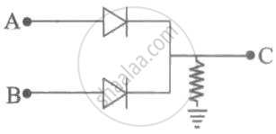
In the circuit below, A and B represent two inputs and C represents the output. The circuit represents ______.
The region near the junction of an unbiased p-n junction diode is known as depletion layer. The layer is depleted of ______.
In a forward bias arrangement of a p-n junction diode, the ______.
At 0.3 V and 0.7 V, the diodes Ge and Si become conductors respectively. In the given figure, if the ends of diode Ge are overturned, the change in potential V0 will be ______.

