Advertisements
Advertisements
Question
Describe briefly with the help of a circuit diagram, how the flow of current carriers in a p-n-p transistor is regulated with emitter-base junction forward biased and base-collector junction reverse biased.
Solution
In p−n−p transistor : →
The emitter base junction is always forward biased with voltage VEE and the collector base junction is always reverse biased with voltage VCC.
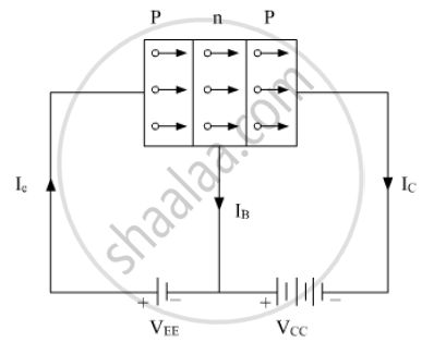
The holes in the emitter are pushed into the base by the positive terminal of battery of voltage VEE. Since, base is thin and lightly doped so only few holes combine with electrons in the base. Thus, base current IB is small. Since VCC is quite large almost 99% of holes coming from emitter are collected by collector. For each hole reaching the collector, an electron is released from the negative terminal of the collector base battery to neutralize the hole. For each hole consumed in collector, a bond breaks in emitter and electron is released that enters positive terminal of emitter-base battery. Thus, we can say the current is carried by holes inside the transistor and by electrons in external circuit.
RELATED QUESTIONS
For transistor action, which of the following statements are correct:
(a) Base, emitter and collector regions should have similar size and doping concentrations.
(b) The base region must be very thin and lightly doped.
(c) The emitter junction is forward biased and collector junction is reverse biased.
(d) Both the emitter junction as well as the collector junction are forward biased.
With the help of circuit diagram explain the working principle of a transistor amplifier as an oscillator.
In oscillatory circuit, reactive components are connected in
