Advertisements
Advertisements
Question
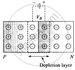
In the depletion region of a diode ______.
- there are no mobile charges.
- equal number of holes and electrons exist, making the region neutral.
- recombination of holes and electrons has taken place.
- immobile charged ions exist.
Options
a and b
a, b and d
c and d
a, b, c and d
Solution
a, b, c and d
Explanation:
On account of the difference in concentration of charge carrier in the two sections of the P-N junction, the electrons from N-region diffuse through the junction into P-region and the hole from P-region diffuse into N-region.

Due to diffusion, the neutrality of both N and P-type semiconductor is disturbed, a layer of negatively charged ions appear near the junction in the P-crystal and a layer of positive ions appears near the junction in N-crystal. This layer is called the depletion layer.
The thickness of the depletion layer is 1 micron = 10-6 m.
Width of depletion layer ∞ 1/Dopping
Depletion is directly proportional to temperature.
Important point: The P-N junction diode is equivalent to the capacitor in which the depletion layer acts as a dielectric.
APPEARS IN
RELATED QUESTIONS
Show on a graph, the variation of resistivity with temperature for a typical semiconductor.
A triode value operates at Vp = 225 V and Vg = −0.5 V.
The plate current remains unchanged if the plate voltage is increased to 250 V and the grid voltage is decreased to −2.5 V. Calculate the amplification factor.
The drift current in a p-n junction is from the ______.
A – pn junction has a depletion layer of thickness .of the order of
When we apply reverse biased to a junction diode, it
Avalanche breakdown is due to ______.
A Zener of power rating 1 W is to be used as a voltage regulator. If zener has a breakdown of 5 V and it has to regulate voltage which fluctuated between 3 V and 7 V, what should be the value of Rs for safe operation (Figure)?

Differentiate between the threshold voltage and the breakdown voltage for a diode.
With reference to a semiconductor diode, define the potential barrier.
What is meant by forward biasing of a semiconductor diode?
