Advertisements
Advertisements
Question
With reference to a semiconductor diode, define the potential barrier.
Solution
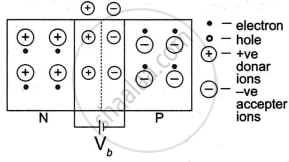
The barrier that the repelling forces use to stop the mobile charge carriers (at the PN junction) is known as the potential barrier.

This results from the concentration of immobile charges close to the junction after electrons and holes diffuse across the function.
APPEARS IN
RELATED QUESTIONS
Draw a labelled diagram of a full wave rectifier. Show how output voltage varies with time if the input voltage is a sinusoidal voltage.
The plate current in a diode is 20 mA when the plate voltage is 50 V or 60 V. What will be the current if the plate voltage is 70 V?
Answer the following question.
Why photodiodes are required to operate in reverse bias? Explain.
Basic materials used in the present solid state electronic devices like diode, transistor, ICs, etc are ______.
The drift current in a p-n junction is from the ______.
In forward bias width of potential barrier in a p + n junction diode
Avalanche breakdown is due to ______.
In the circuit shown in figure, if the diode forward voltage drop is 0.3 V, the voltage difference between A and B is ______.

Consider an npn transistor with its base-emitter junction forward biased and collector base junction reverse biased. Which of the following statements are true?
- Electrons crossover from emitter to collector.
- Holes move from base to collector.
- Electrons move from emitter to base.
- Electrons from emitter move out of base without going to the collector.
Can the potential barrier across a p-n junction be measured by simply connecting a voltmeter across the junction?
