Advertisements
Advertisements
Question
With reference to a semiconductor diode, define the depletion region.
Solution
A semiconductor diode's depletion zone is the area surrounding the p-n junction where there are no mobile charge carriers, this area generates an electric field that allows the diode to conduct in one direction while blocking in another.
APPEARS IN
RELATED QUESTIONS
(i) Explain with the help of a diagram the formation of depletion region and barrier potential in a pn junction.
With the help of neat labelled circuit diagram explain the working of half wave rectifier using semiconductor diode. Draw the input and output waveforms.
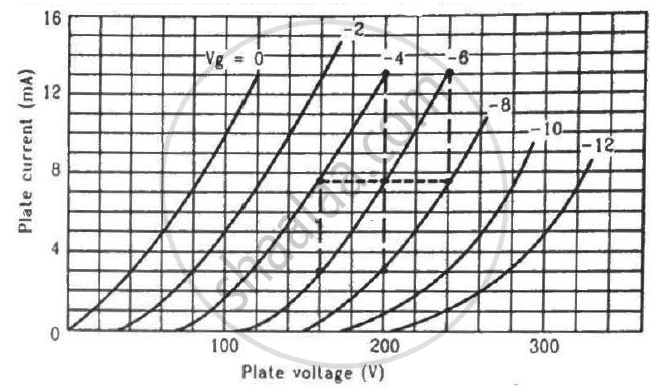
Find the values of rp, µ and gm of a triode operating at plate voltage 200 V and grid voltage −6. The plate characteristics are shown in the figure.
Diffusion in a p-n junction is due to ______.
Of the diodes shown in the following diagrams, which one is reverse biased?
When we apply reverse biased to a junction diode, it
When an electric field is applied across a semiconductor ______.
- electrons move from lower energy level to higher energy level in the conduction band.
- electrons move from higher energy level to lower energy level in the conduction band.
- holes in the valence band move from higher energy level to lower energy level.
- holes in the valence band move from lower energy level to higher energy level.
The breakdown in a reverse biased p–n junction diode is more likely to occur due to ______.
- large velocity of the minority charge carriers if the doping concentration is small.
- large velocity of the minority charge carriers if the doping concentration is large.
- strong electric field in a depletion region if the doping concentration is small.
- strong electric field in the depletion region if the doping concentration is large.
Draw V-I characteristics of a p-n Junction diode.
What is meant by forward biasing of a semiconductor diode?
