Advertisements
Advertisements
प्रश्न
Derive the expression for the voltage gain of a transistor amplifier in CE configuration in terms of the load resistance RL, current gain a βa and input resistance.
Explain why input and output voltages are in opposite phase.
उत्तर
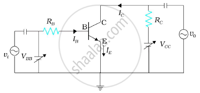
To operate the transistor as an amplifier it is necessary to fix its operating point somewhere in the middle of its active region. If we fix the value of VBB corresponding to a point in the middle of the linear part of the transfer curve then the dc base current IB would be constant and corresponding collector current IC will also be constant. The dc voltage VCE = VCC - ICRC would also remain constant. The operating values of VCE and IB determine the operating point, of the amplifier.

If a small sinusoidal voltage with amplitude vs is superposed on the dc base bias by connecting the source of that signal in series with the VBB supply, then the base current will have sinusoidal variations superimposed on the value of IB. As a consequence the collector current also will have sinusoidal variations superimposed on the value of IC, producing in turn corresponding change in the value of VO. We can measure the ac variations across the input and output terminals by blocking the dc voltages by large capacitors.
In the discription of the amplifier given above we have not considered any ac signal. In general, amplifiers are used to amplify alternating signals. Now let us superimpose an ac input signal vi (to be amplified) on the bias VBB (dc) as shown in figure. The output is taken between the collector and the ground.
The working of an amplifier can be easily understood, if we first assume that vi = 0. Then applying Kirchhoff’s law to the output loop, we get
Vcc = VCE + Ic RL ——— (i)
Likewise, the input loop gives
VBB = VBE + IB RB ——— (ii)
When vi is not zero, we get
VBB + vi = (VBE + ΔVBE) + (IB + ΔIB)RB
Or , VBB + vi = VBE + IB RB + ΔVBE + ΔIBRB
The change in VBE can be related to the input resistance ri and the change in IB as Δ VBE = ΔIB ri
So we get, VBB + vi = VBE + IB RB + ΔIB(RB + ri) —— (iii)
Subtracting (ii) from (iii) we get
vi = ΔIB (RB + ri) = r ΔIB ——— (iv)
The change in IB causes a change in Ic. We define a parameter βac, which is similar to the βdc, as
`beta_ac = (Delta I_c)/(Delta I_B) = (i_c)/(i_b) ` ——— (v)
which is also known as the ac current gain Ai. Usually βac, is close to βdc in the linear region of the output characteristics.
The change in Ic due to a change in IB causes a change in VCE and the voltage drop across the resistor RL because VCC is fixed.
These changes can be given by Eq. (i) as
ΔVCC = ΔVCE + RL ΔIC = 0
or ΔVCE = –RL ΔIC
The change in VCE is the output voltage v0. From Eq. (v), we get
v0 = ΔVCE = - βac RL ΔlB ——— (vi)
The voltage gain of the amplifier is
`A_v = (v_0)/(v_i) = (Delta V_(CE))/(rDelta I_B) = (-beta _(ac) R_L)/r` {using eq. (iv) and (vi) }
The negative sign represents that output voltage is opposite in phase with the input voltage.
APPEARS IN
संबंधित प्रश्न
Draw a simple circuit of a CE transistor amplifier. Explain its working ?
Show that the voltage gain, AV, of the amplifier is given by `A_v = (beta_(ac) R_1)/r_i`where βac is the current gain, RL is the load resistance and ri is the input resistance of the transistor. What is the significance of the negative sign in the expression for the voltage gain?
Let iE, iC and iB represent the emitter current, the collector current and the base current respectively in a transistor. Then
(a) iC is slightly smaller than iE
(b) iC is slightly greater than iE
(c) iB is much smaller than iE
(d) iB is much greater than iE.
In a normal operation of a transistor,
(a) the base−emitter junction is forward-baised
(b) the base−collector junction is forward-baised
(c) the base−emitter junction is reverse-baised
(d) the base−collector junction is reverse-baised.
Draw a circuit diagram of an n-p-n transistor with its emitter-base junction forward biased and basecollector junction reverse biased. Briefly describe its working.
Explain how a transistor in its active state exhibits a low resistance at its emitter-base junction and high resistance at its base-collector junction.
Draw a circuit diagram of an n-p-n transistor with its emitter-base junction forward biased and base-collector junction reverse biased. Briefly describe its working.
Explain how a transistor in its active state exhibits a low resistance at its emitter-base junction and high resistance at its base-collector junction.
Derive the expression for the voltage gain of a transistor amplifier in CE configuration in terms of the load resistance RL, current gain βa and input resistance.
Explain why input and output voltages are in the opposite phase.
Answer the following question.
Draw the circuit arrangement for studying the output characteristics of an n-p-n transistor in CE configuration. Explain how the output characteristics is obtained.
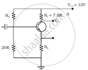
For the transistor circuit shown in figure, evaluate VE, RB, RE given IC = 1 mA, VCE = 3 V, VBE = 0.5 V and VCC = 12 V, β = 100.

