Advertisements
Advertisements
प्रश्न
Let iE, iC and iB represent the emitter current, the collector current and the base current respectively in a transistor. Then
(a) iC is slightly smaller than iE
(b) iC is slightly greater than iE
(c) iB is much smaller than iE
(d) iB is much greater than iE.
उत्तर
(a) iC is slightly smaller than iE
(c) iB is much smaller than iE
The highlighted parts could not be edited, as the meaning could not be understood. Also, please check the last line for logical accuracy. Only one option is given as correct, while the solution gives two correct options.
We know that in the transistor base is slightly doped, therefore when the majority carriers due to forward biasing of emitter base junction, feel the repulsive force from the battery and pass over to the base region. This gives the emitter current iE.
As the base is thin and lightly doped, only few majority carriers of the emitter are neutralised at the base. This gives the base current. Hence, base current `( i_B)` is low.
The remaining majority carriers of the emitter pass to the collector and give collector current iC.
Thus, we get the relation given below:
iE = iB + iC
Thus, because of the base, current iC is slightly smaller than iE .
Hence, option (a) and (c) are correct.
APPEARS IN
संबंधित प्रश्न
Draw a simple circuit of a CE transistor amplifier. Explain its working ?
Show that the voltage gain, AV, of the amplifier is given by `A_v = (beta_(ac) R_1)/r_i`where βac is the current gain, RL is the load resistance and ri is the input resistance of the transistor. What is the significance of the negative sign in the expression for the voltage gain?
In a normal operation of a transistor,
(a) the base−emitter junction is forward-baised
(b) the base−collector junction is forward-baised
(c) the base−emitter junction is reverse-baised
(d) the base−collector junction is reverse-baised.
Draw a circuit diagram of an n-p-n transistor with its emitter-base junction forward biased and basecollector junction reverse biased. Briefly describe its working.
Explain how a transistor in its active state exhibits a low resistance at its emitter-base junction and high resistance at its base-collector junction.
Derive the expression for the voltage gain of a transistor amplifier in CE configuration in terms of the load resistance RL, current gain a βa and input resistance.
Explain why input and output voltages are in opposite phase.
Draw a circuit diagram of an n-p-n transistor with its emitter-base junction forward biased and base-collector junction reverse biased. Briefly describe its working.
Explain how a transistor in its active state exhibits a low resistance at its emitter-base junction and high resistance at its base-collector junction.
Derive the expression for the voltage gain of a transistor amplifier in CE configuration in terms of the load resistance RL, current gain βa and input resistance.
Explain why input and output voltages are in the opposite phase.
Answer the following question.
Draw the circuit arrangement for studying the output characteristics of an n-p-n transistor in CE configuration. Explain how the output characteristics is obtained.
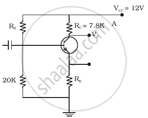
For the transistor circuit shown in figure, evaluate VE, RB, RE given IC = 1 mA, VCE = 3 V, VBE = 0.5 V and VCC = 12 V, β = 100.

