Advertisements
Advertisements
प्रश्न
Draw the circuit diagram of a half wave rectifier and explain its working.
Explain, with the help of a circuit diagram, the working of a p-n junction diode as a half-wave rectifier.
उत्तर
The circuit diagram for a half wave rectifier is shown below:

Working:
During the positive half cycle of the input a.c., the p-n junction is forward biased i.e the forward current flows from p to n and the diode offers a low resistance path to the current. Thus, we get output across-load i.e. a.c input will be obtained as d.c output.
During the negative half cycle of the input a.c., the p-n junction is reversed biased i.e the reverse current flows from n to p, the diode offers a high resistance path to the current. Thus, we get no output across-load. This principle is shown in the diagram given below.

APPEARS IN
संबंधित प्रश्न
Draw the circuit diagram of a full wave rectifier. Explain its working showing its input and output waveforms.
Briefly explain how the output voltage/current is unidirectional.
When the diode shows saturated current, dynamic place resistance is _____________ .
Fill in the blank.
The ability of a junction diode to __________ an alternating voltage is based on the fact that it allows current to pass only when it is forward biased.
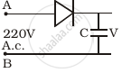
A 220 V A.C. supply is connected between points A and B (figure). What will be the potential difference V across the capacitor?
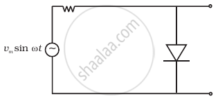
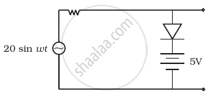
The output of the given circuit in figure is given below.
To reduce the ripples in a rectifier circuit with capacitor filter ______.
- RL should be increased.
- input frequency should be decreased.
- input frequency should be increased.
- capacitors with high capacitance should be used.
Assuming the ideal diode, draw the output waveform for the circuit given in figure. Explain the waveform.
With the help of a circuit diagram, explain briefly how a p-n junction diode works as a half-wave rectifier.
Give two differences between a half-wave rectifier and a full-wave rectifier.
