Advertisements
Advertisements
प्रश्न
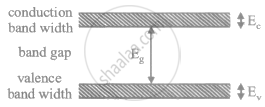
Let ΔE denote the energy gap between the valence band and the conduction band. The population of conduction electrons (and of the holes) is roughly proportional to e−ΔE/2kT. Find the ratio of the concentration of conduction electrons in diamond to the in silicon at room temperature 300 K. ΔE for silicon is 1.1 eV and for diamond is 6.1 eV. How many conduction electrons are likely to be in one cubic metre of diamond?
उत्तर
Given:
Number of electrons in the conduction band, n = e−ΔE/2kT
Band gap of diamond, ΔE1 = 6 eV
Band gap of silicon, ΔE2 = 1.1 eV
Now,
\[n_{\text{ diamond}} = e^\frac{- \Delta E_1}{2\text{ kT}} \]
\[ n_{\text{ silicon}} = e^\frac{- \Delta E_2}{2\text{ kT}} \]
\[ \therefore \frac{n_{\text{ diamond }}}{n_{\text{ silicon}}} = e^\frac{- 1}{2kT}( ∆ E_1 - ∆ E_2 ) \]
\[ \Rightarrow \frac{n_{\text{diamond}}}{n_{\text{silicon}}} = e^\frac{- 1}{2 \times 8 . 62 \times {10}^{- 5} \times 300}(6 . 0 - 1 . 1) \]
\[ \Rightarrow \frac{n_{\text{diamond}}}{n_{\text{silicon}}} = 7 . 15 \times {10}^{- 42}\]
Because of more band gap, the conduction electrons per cubic metre in diamond are very less as compared to those in silicon, or we can simply say that they are almost zero.
APPEARS IN
संबंधित प्रश्न
Write two characteristic features to distinguish between n-type and p-type semiconductors ?
There are energy bands in a solid. Do we have really continuous energy variation in a band ro do we have very closely spaced but still discrete energy levels?
The conduction band of a solid is partially filled at 0 K. Will it be a conductor, a semiconductor or an insulator?
When an electron goes from the valence band to the conduction band in silicon, its energy is increased by 1.1 eV. The average energy exchanged in a thermal collision is of the order of kT which is only 0.026 eV at room temperature. How is a thermal collision able to take some to the electrons from the valence band to the conduction band?
What is the resistance of an intrinsic semiconductor at 0 K?
We have valence electrons and conduction electrons in a semiconductor. Do we also have 'valence holes' and 'conduction holes'?
An electric field is applied to a semiconductor. Let the number of charge carries be nand the average drift speed by v. If the temperature is increased,
The electrical conductivity of pure germanium can be increased by
(a) increasing the temperature
(b) doping acceptor impurities
(c) doping donor impurities
(d) irradiating ultraviolet light on it.
The band gap for silicon is 1.1 eV. (a) Find the ratio of the band gap to kT for silicon at room temperature 300 K. (b) At what temperature does this ratio become one tents of the value at 300 K? (Silicon will not retain its structure at these high temperatures.)
(Use Planck constant h = 4.14 × 10⁻¹⁵ eV-s, Boltzmann constant k = 8·62 × 10-5 eV/K.)
When a semiconducting material is doped with an impurity, new acceptor levels are created. In a particular thermal collision, a valence electron receives an energy equal to 2kT and just reaches one of the acceptor levels. Assuming that the energy of the electron was at the top edge of the valence band and that the temperature T is equal to 300 K, find the energy of the acceptor levels above the valence band.
Suppose the energy liberated in the recombination of a hole-electron pair is converted into electromagnetic radiation. If the maximum wavelength emitted is 820 nm, what is the band gap?
(Use Planck constant h = 4.14 × 10⁻¹⁵ eV-s, Boltzmann constant k = 8·62 × 10-5 eV/K.)
A semiconducting material has a band gap of 1 eV. Acceptor impurities are doped into it which create acceptor levels 1 meV above the valence band. Assume that the transition from one energy level to the other is almost forbidden if kT is less than 1/50 of the energy gap. Also if kT is more than twice the gap, the upper levels have maximum population. The temperature of the semiconductor is increased from 0 K. The concentration of the holes increases with temperature and after a certain temperature it becomes approximately constant. As the temperature is further increased, the hole concentration again starts increasing at a certain temperature. Find the order of the temperature range in which the hole concentration remains approximately constant.
(Use Planck constant h = 4.14 × 10⁻¹⁵ eV-s, Boltzmann constant k = 8·62 × 10-5 eV/K.)
Hydrogen atom in n = 3 state has a lifetime of 10-10 sec. The number of revolutions an electron makes in the n = 3 state before returning to the ground state is ______.
Useful data
`1/(4pi∈_0) = 8.99 xx 10^-34`N m2 C-2; e = 1.60 10-19 C; h = 6.63 10-34 Js; me = 9 × 10⁻³ kg
If the lattice constant of this semiconductor is decreased, then which of the following is correct?

An n-type semiconductor is
For germanium crystal, the forbidden gas energy gap
In a semiconductor, the forbidden energy gap between the valence, band and the conduction band is of the order of
The valance of an impurity added to germanium crystal in order to convert it into p-type semiconductor is
- Assertion (A): In insulators, the forbidden gap is very large.
- Reason (R): The valence electrons in an atom of an insulator are very tightly bound to the nucleus.
