Advertisements
Advertisements
प्रश्न
What is meant by forward biasing of a semiconductor diode?
उत्तर
When the positive terminal of an external battery is connected to the n-region of the diode and the negative terminal is connected to the same n-region, the diode is said to be forward biased.
APPEARS IN
संबंधित प्रश्न
(i) Explain with the help of a diagram the formation of depletion region and barrier potential in a pn junction.
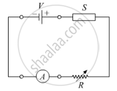
In the following diagram 'S' is a semiconductor. Would you increase or decrease the value of R to keep the reading of the ammeter A constant when S is heated? Give reason for your answer.

We use alloys for making standard resistors because they have ____________.
Of the diodes shown in the following diagrams, which one is reverse biased?
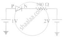
The current through an ideal PN-junction shown in the following circuit diagram will be:

In the depletion region of a diode ______.
- there are no mobile charges.
- equal number of holes and electrons exist, making the region neutral.
- recombination of holes and electrons has taken place.
- immobile charged ions exist.
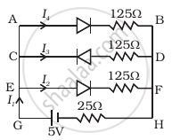
If each diode in figure has a forward bias resistance of 25 Ω and infinite resistance in reverse bias, what will be the values of the current I1, I2, I3 and I4?

The graph of potential barrier versus width of depletion region for an unbiased diode is shown in graph A. In comparison to A, graphs B and C are obtained after biasing the diode in different ways. Identify the type of biasing in B and C and justify your answer
| ‘A’ | ‘B’ | ‘C’ |
 |
 |
 |
Draw V-I characteristics of a p-n Junction diode.
Answer the following giving reasons:
A p-n junction diode is damaged by a strong current.
