Advertisements
Advertisements
प्रश्न
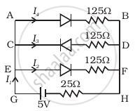
If each diode in figure has a forward bias resistance of 25 Ω and infinite resistance in reverse bias, what will be the values of the current I1, I2, I3 and I4?
उत्तर
According to the problem, forward biased resistance = 25 Ω and reverse biased resistance = ∞
As shown in the figure, the diode in branch CD is in reverse biased which has infinite resistance.
So, the current in that branch is zero, i.e. I3, = 0
Resistance in branch AB = 25 + 125 = 150 Ω say R1
Resistance in branch EF = 25 + 125 = 150 Ω, say R2
AB is parallel to EF
So, effective resistance
`1/R^' = 1/R_1 + 1/R_2 = 1/150 + 1/150 = 2/150`
⇒ R' 75 Ω
Total resistance R of the circuit = R' + 25 = 75 + 25 = 100 Ω
Current `I_1 = V/R = 5/100` = 0.05 A
According to Kirchhoff's, current law (KCL),
I1 = I4 + I2 + I3 .....(Here I3 = 0)
So I1 = I4 + I2
Here, the resistance R1 and R2 are same.
i.e., I4 = I2
∴ I1 = 2I2
⇒ `I_2 = I_1/2 = 0.05/2` = 0.025 A
And I4 = 0.025 A
Therefore, we get, I1 = 0.05 A, I2 = 0.025 A, I3 = 0 and I4 = 0.025 A.
APPEARS IN
संबंधित प्रश्न
(i) Explain with the help of a diagram the formation of depletion region and barrier potential in a pn junction.
What causes the setting up of high electric field even for small reverse bias voltage across the diode?
With reference to semi-conductors answer the following :
(i) What is the change in the resistance of the semi-conductor with increase in temperature ?
(ii) Name the majority charge carriers in n-type semi-conductor.
(iii) What is meant by doping ?
We use alloys for making standard resistors because they have ____________.
With reference to Semiconductor Physics,
Name the diode that emits spontaneous radiation when forward biased.
When we apply reverse biased to a junction diode, it
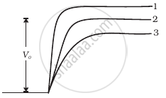
In Figure, Vo is the potential barrier across a p-n junction, when no battery is connected across the junction ______.
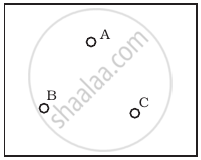
Consider a box with three terminals on top of it as shown in figure (a):
 (a) |
Three components namely, two germanium diodes and one resistor are connected across these three terminals in some arrangement. A student performs an experiment in which any two of these three terminals are connected in the circuit shown in figure (b).
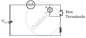 (b) |
The student obtains graphs of current-voltage characteristics for unknown combination of components between the two terminals connected in the circuit. The graphs are
(i) when A is positive and B is negative
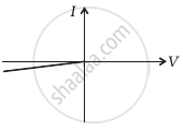 (c) |
(ii) when A is negative and B is positive
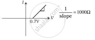 (d) |
(iii) When B is negative and C is positive
|
(e) |
(iv) When B is positive and C is negative
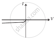 (f) |
(v) When A is positive and C is negative
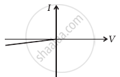 (g) |
(vi) When A is negative and C is positive
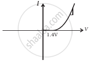 (h) |
From these graphs of current-voltage characteristics shown in figure (c) to (h), determine the arrangement of components between A, B and C.
Draw the circuit arrangement for studying V-I characteristics of a p-n junction diode in (i) forward biasing and (ii) reverse biasing. Draw the typical V-I characteristics of a silicon diode.
What is meant by forward biasing of a semiconductor diode?
