Advertisements
Advertisements
प्रश्न
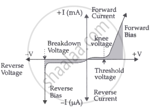
Draw V-I characteristics of a p-n Junction diode.
उत्तर

APPEARS IN
संबंधित प्रश्न
Draw a labelled diagram of a full wave rectifier. Show how output voltage varies with time if the input voltage is a sinusoidal voltage.
Plot a graph showing variation of current versus voltage for the material GaAs ?
Diffusion in a p-n junction is due to ______.
Depletion layer in p - n junction diode consists of
The breakdown in a reverse biased p–n junction diode is more likely to occur due to ______.
- large velocity of the minority charge carriers if the doping concentration is small.
- large velocity of the minority charge carriers if the doping concentration is large.
- strong electric field in a depletion region if the doping concentration is small.
- strong electric field in the depletion region if the doping concentration is large.
Can the potential barrier across a p-n junction be measured by simply connecting a voltmeter across the junction?
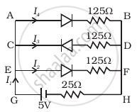
If each diode in figure has a forward bias resistance of 25 Ω and infinite resistance in reverse bias, what will be the values of the current I1, I2, I3 and I4?

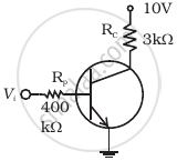
In the circuit shown in figure, when the input voltage of the base resistance is 10 V, Vbe is zero and Vce is also zero. Find the values of Ib, Ic and β.

Write the property of a junction diode which makes it suitable for rectification of ac voltages.
What is meant by forward biasing of a semiconductor diode?
