Advertisements
Advertisements
प्रश्न
Electric conduction in a semiconductor takes place due to
पर्याय
electrons only
holes only
both electrons and holes
neither electrons nor holes.
उत्तर
both electrons and holes
A hole is created in a semiconductor when a valence electron moves to the conduction band. When potential difference is applied across the semiconductor, the electron drifts opposite to the electric field applied, while the hole moves along the electric field. Therefore, electric conduction takes place in a semiconductor because of both electrons and holes.
APPEARS IN
संबंधित प्रश्न
Draw energy band diagrams of an n-type and p-type semiconductor at temperature T > 0 K. Mark the donor and acceptor energy levels with their energies.
The conduction band of a solid is partially filled at 0 K. Will it be a conductor, a semiconductor or an insulator?
When an electron goes from the valence band to the conduction band in silicon, its energy is increased by 1.1 eV. The average energy exchanged in a thermal collision is of the order of kT which is only 0.026 eV at room temperature. How is a thermal collision able to take some to the electrons from the valence band to the conduction band?
An electric field is applied to a semiconductor. Let the number of charge carries be nand the average drift speed by v. If the temperature is increased,
A p-type semiconductor is
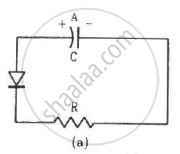
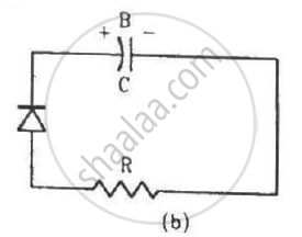
Two identical capacitors A and B are charged to the same potential V and are connected in two circuits at t = 0 as shown in figure. The charges on the capacitors at a time t = CRare, respectively,


In a semiconductor,
(a) there are no free electrons at 0 K
(b) there are no free electrons at any temperature
(c) the number of free electrons increases with temperature
(d) the number of free electrons is less than that in a conductor.
Indium antimonide has a band gap of 0.23 eV between the valence and the conduction band. Find the temperature at which kT equals the band gap.
When a semiconducting material is doped with an impurity, new acceptor levels are created. In a particular thermal collision, a valence electron receives an energy equal to 2kT and just reaches one of the acceptor levels. Assuming that the energy of the electron was at the top edge of the valence band and that the temperature T is equal to 300 K, find the energy of the acceptor levels above the valence band.
The band gap between the valence and the conduction bands in zinc oxide (ZnO) is 3.2 eV. Suppose an electron in the conduction band combines with a hole in the valence band and the excess energy is released in the form of electromagnetic radiation. Find the maximum wavelength that can be emitted in this process.
Let ΔE denote the energy gap between the valence band and the conduction band. The population of conduction electrons (and of the holes) is roughly proportional to e−ΔE/2kT. Find the ratio of the concentration of conduction electrons in diamond to the in silicon at room temperature 300 K. ΔE for silicon is 1.1 eV and for diamond is 6.1 eV. How many conduction electrons are likely to be in one cubic metre of diamond?
Hydrogen atom in n = 3 state has a lifetime of 10-10 sec. The number of revolutions an electron makes in the n = 3 state before returning to the ground state is ______.
Useful data
`1/(4pi∈_0) = 8.99 xx 10^-34`N m2 C-2; e = 1.60 10-19 C; h = 6.63 10-34 Js; me = 9 × 10⁻³ kg
The energy of a hydrogen atom in the ground state is −13.6 eV. The energy of a He+ ion in the first excited state will be:
An n-type semiconductor is
The valance of an impurity added to germanium crystal in order to convert it into p-type semiconductor is
The reaction between α and β parameter of a transistor is given by
Hole are majority charge carrier in
