Advertisements
Advertisements
प्रश्न
A p-type semiconductor is
पर्याय
positively charged
negatively charged
uncharged
uncharged at O K but charged at higher temperatures.
उत्तर
uncharged
A p-type semiconductor is formed by doping a pure semiconductor with a p-type material. As impurity atoms take the position of the germanium atom in a germanium crystal, three electrons of a p-type material form covalent bonds by sharing electrons with three neighbouring germanium atoms. However, the fourth covalent bond is left incomplete, with a want of one electron. This creates a hole. As the atom as a whole is neutral, the p-type material is also neutral.
APPEARS IN
संबंधित प्रश्न
Distinguish between a conductor and a semi conductor on the basis of energy band diagram
Draw energy band diagrams of an n-type and p-type semiconductor at temperature T > 0 K. Mark the donor and acceptor energy levels with their energies.
There are energy bands in a solid. Do we have really continuous energy variation in a band ro do we have very closely spaced but still discrete energy levels?
What is the resistance of an intrinsic semiconductor at 0 K?
An electric field is applied to a semiconductor. Let the number of charge carries be nand the average drift speed by v. If the temperature is increased,
When an impurity is doped into an intrinsic semiconductor, the conductivity of the semiconductor
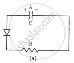
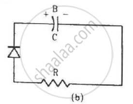
Two identical capacitors A and B are charged to the same potential V and are connected in two circuits at t = 0 as shown in figure. The charges on the capacitors at a time t = CRare, respectively,


An incomplete sentence about transistors is given below:
The emitter−..... junction is __ and the collector−..... junction is __. The appropriate words for the dotted empty positions are, respectively,
In a pure semiconductor, the number of conduction election 6 × 10¹⁹ per cubic metre. How many holes are there in a sample of size 1 cm × 1 mm?
When a semiconducting material is doped with an impurity, new acceptor levels are created. In a particular thermal collision, a valence electron receives an energy equal to 2kT and just reaches one of the acceptor levels. Assuming that the energy of the electron was at the top edge of the valence band and that the temperature T is equal to 300 K, find the energy of the acceptor levels above the valence band.
Suppose the energy liberated in the recombination of a hole-electron pair is converted into electromagnetic radiation. If the maximum wavelength emitted is 820 nm, what is the band gap?
(Use Planck constant h = 4.14 × 10⁻¹⁵ eV-s, Boltzmann constant k = 8·62 × 10-5 eV/K.)
Estimate the proportion of boron impurity which will increase the conductivity of a pure silicon sample by a factor of 100. Assume that each boron atom creates a hole and the concentration of holes in pure silicon at the same temperature is 7 × 10¹⁵ holes per cubic metre. Density of silicon 5 × 1028 atoms per cubic metre.
A hole in a. p – type semiconductor is
For germanium crystal, the forbidden gas energy gap
A semiconductor is cooled from T.K to T2K its resistance will
In a semiconductor, the forbidden energy gap between the valence, band and the conduction band is of the order of
The valance of an impurity added to germanium crystal in order to convert it into p-type semiconductor is
The energy required by an electron to jump the forbidden band in silicon at room temperature is about ______.
